Datasheet4U Logo Datasheet4U.com

ICS950201 - Programmable Timing Controller

Datasheet Summary

Description

PIN NUMBER 1, 8, 14, 19, 26, 32, 37, 46, 50 2 PIN NAME VDD X1 3 X2 7, 6, 5 4, 9, 15, 20, 27, 31, 36, 41, 47 18, 17, 16, 13, 12,11, 10 24,23, 22, 21 24 25 PCICLK_F (2:0) GND PCICLK (6:0) 3V66 (5:2) 3V66_5 PD# 28 Vtt_PWRGD# 29 SDATA 30 SCLK 33 3V66_0 34 PCI_STOP# 35 38 39 40 , 42 43 44, 48, 51

Features

  • 3 Differential CPU Clock Pairs @ 3.3V.
  • 7 PCI (3.3V) @ 33.3MHz.
  • 3 PCI_F (3.3V) @ 33.3MHz.
  • 1 USB (3.3V) @ 48MHz.
  • 1 DOT (3.3V) @ 48MHz.
  • 1 REF (3.3V) @ 14.318MHz.
  • 5 3V66 (3.3V) @ 66.6MHz.
  • 1 VCH/3V66 (3.3V) @ 48MHz or 66.6MHz Features:.
  • Supports spread spectrum modulation, down spread 0 to -0.5%.
  • Efficient power management scheme through PD#, CPU_STOP# and PCI_STOP#.
  • Uses external 14.318MHz crystal.

📥 Download Datasheet

Datasheet preview – ICS950201

Datasheet Details

Part number ICS950201
Manufacturer Renesas
File Size 312.54 KB
Description Programmable Timing Controller
Datasheet download datasheet ICS950201 Datasheet
Additional preview pages of the ICS950201 datasheet.
Other Datasheets by Renesas

Full PDF Text Transcription

Click to expand full text
DATASHEET Programmable Timing Control HubTM for P4TM ICS950201 Recommended Application: CK-408 clock for Intel® 845 chipset with P4 processor. Output Features: • 3 Differential CPU Clock Pairs @ 3.3V • 7 PCI (3.3V) @ 33.3MHz • 3 PCI_F (3.3V) @ 33.3MHz • 1 USB (3.3V) @ 48MHz • 1 DOT (3.3V) @ 48MHz • 1 REF (3.3V) @ 14.318MHz • 5 3V66 (3.3V) @ 66.6MHz • 1 VCH/3V66 (3.3V) @ 48MHz or 66.6MHz Features: • Supports spread spectrum modulation, down spread 0 to -0.5%. • Efficient power management scheme through PD#, CPU_STOP# and PCI_STOP#. • Uses external 14.318MHz crystal • Stop clocks and functional control available through I2C interface. Key Specifications: • CPU Output Jitter <150ps • 3V66 Output Jitter <250ps • CPU Output Skew <100ps, programmable over 800 ps with groups CPU0,1 and CPU2.
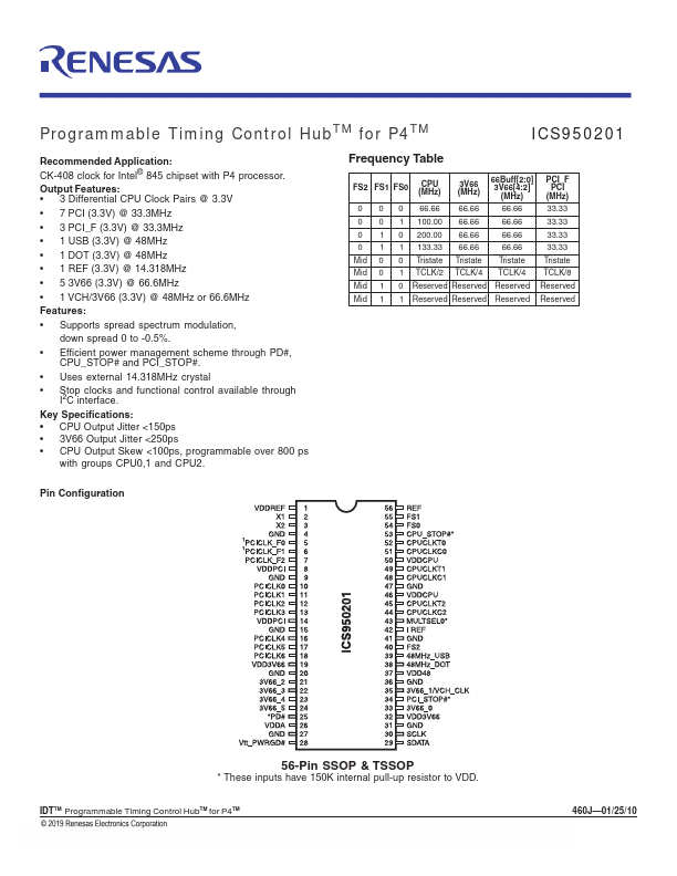
Published: |