ICS97U8770
ICS97U8770 is 1.8V Wide Range Frequency Clock Driver manufactured by Renesas.
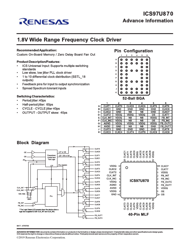
ICS97U870
Advance Information
Pin Descriptions
Terminal Name
AGND
AVDD CLK_INT CLK_INC FB_INT FB_INC FB_OUTT FB_OUTC
Description
Analog Ground Analog power Clock input with a (10K-100K Ohm) pulldown resistor plentary clock input with a (10K-100K Ohm) pulldown resistor Feedback clock input plementary feedback clock input Feedback clock output plementary feedback clock output
OE OS
VDDQ CLKT[0:9] CLKC[0:9]
Output Enable (Asynchronous) Output Select (tied to GND or V000) Ground Logic and output power Clock outputs plementary clock outputs No ball
Electrical Characteristics Ground 1.8 V nominal Differential input Differential input Differential input Differential input...