Datasheet Summary
Low Skew Output Buffer
General Description
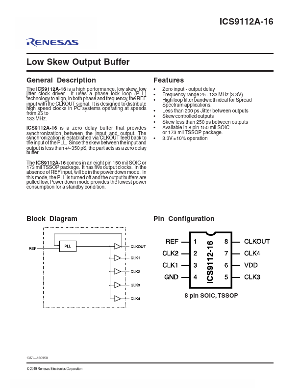
The ICS9112A-16 is a high performance, low skew, low jitter clock driver. It uses a phase lock loop (PLL) technology to align, in both phase and frequency, the REF input with the CLKOUT signal. It is designed to distribute high speed clocks in PC systems operating at speeds from 25 to 133 MHz.
ICS9112A-16 is a zero delay buffer that provides synchronization between the input and output. The synchronization is established via CLKOUT feed back to the input of the PLL. Since the skew between the input and output is less than +/- 350 pS, the part acts as a zero delay buffer.
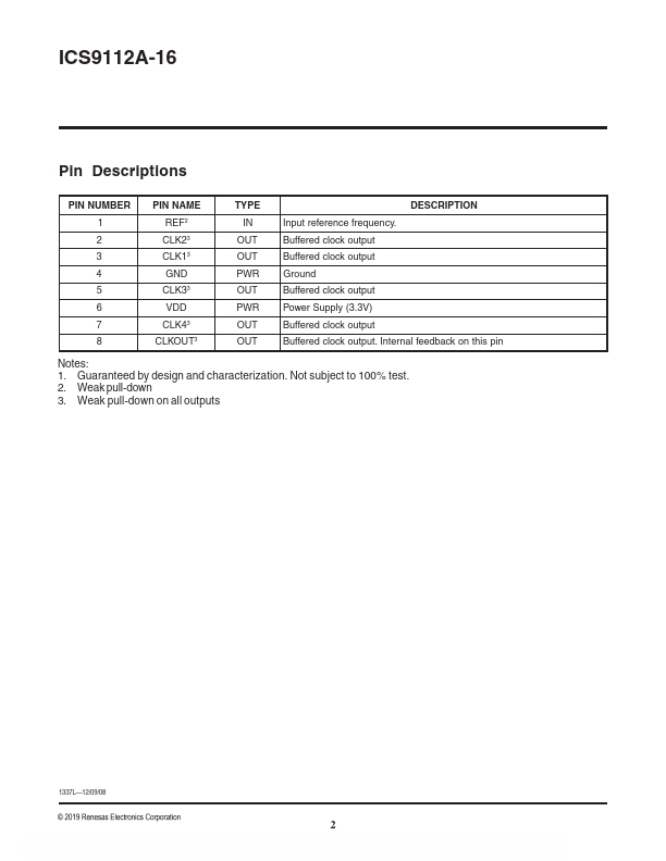
The ICS9112A-16 es in an eight pin 150 mil SOIC or 173...