Datasheet4U Logo Datasheet4U.com

IDT49FCT3805 - CMOS BUFFER/CLOCK DRIVER

Datasheet Summary

Description

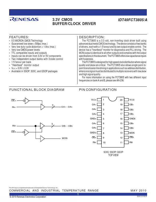
The FCT3805 is a 3.3 volt, non-inverting clock driver built using advanced dual metal CMOS technology.

The device consists of two banks of drivers, each with a 1:5 fanout and its own output enable control.

The device has a "heartbeat" monitor for diagnostics and PLL driving.

Features

  • 0.5 MICRON CMOS Technology.
  • Guaranteed low skew < 500ps (max. ).
  • Very low duty cycle distortion < 1.0ns (max. ).
  • Very low CMOS power levels.
  • TTL compatible inputs and outputs.
  • Inputs can be driven from 3.3V or 5V components.
  • Two independent output banks with 3-state control.
  • 1:5 fanout per bank.
  • "Heartbeat" monitor output.
  • VCC = 3.3V ± 0.3V.
  • Available in SSOP, SOIC, and QSOP packages.

📥 Download Datasheet

Datasheet preview – IDT49FCT3805

Datasheet Details

Part number IDT49FCT3805
Manufacturer Renesas
File Size 195.99 KB
Description CMOS BUFFER/CLOCK DRIVER
Datasheet download datasheet IDT49FCT3805 Datasheet
Additional preview pages of the IDT49FCT3805 datasheet.
Other Datasheets by Renesas

Full PDF Text Transcription

Click to expand full text
IDT49FCT3805/A 3.3V CMOS BUFFER/CLOCK DRIVER COMMERCIAL AND INDUSTRIAL TEMPERATURE RANGE 3.3V CMOS BUFFER/CLOCK DRIVER IDT49FCT3805/A FEATURES: • 0.5 MICRON CMOS Technology • Guaranteed low skew < 500ps (max.) • Very low duty cycle distortion < 1.0ns (max.) • Very low CMOS power levels • TTL compatible inputs and outputs • Inputs can be driven from 3.3V or 5V components • Two independent output banks with 3-state control • 1:5 fanout per bank • "Heartbeat" monitor output • VCC = 3.3V ± 0.3V • Available in SSOP, SOIC, and QSOP packages FUNCTIONAL BLOCK DIAGRAM DESCRIPTION: The FCT3805 is a 3.3 volt, non-inverting clock driver built using advanced dual metal CMOS technology. The device consists of two banks of drivers, each with a 1:5 fanout and its own output enable control.
Published: |