Datasheet4U Logo Datasheet4U.com

MPC9447 - LVCMOS Clock Fanout Buffer

Description

MPC9447 is specifically designed to distribute LVCMOS compatible clock signals up to a frequency of 350 MHz.

Each output provides a precise copy of the input signal with a near zero skew.

The outputs buffers support driving of 50  terminated transmission lines on the incident edge.

Features

  • 9 LVCMOS Compatible Clock Outputs.
  • 2 Selectable, LVCMOS Compatible Inputs.
  • Maximum Clock Frequency of 350 MHz.
  • Maximum Clock Skew of 150 ps.
  • Synchronous Output Stop in Logic Low State Eliminates Output Runt Pulses.
  • High-Impedance Output Control.
  • 3.3 V or 2.5 V Power Supply.
  • Drives up to 18 Series Terminated Clock Lines.
  • Ambient Temperature Range -40C to +85C.
  • 32-Lead LQFP Packaging, Pb-free.
  • Sup.

📥 Download Datasheet

Datasheet preview – MPC9447

Datasheet Details

Part number MPC9447
Manufacturer Renesas
File Size 291.98 KB
Description LVCMOS Clock Fanout Buffer
Datasheet download datasheet MPC9447 Datasheet
Additional preview pages of the MPC9447 datasheet.
Other Datasheets by Renesas

Full PDF Text Transcription

Click to expand full text
3.3V, 2.5V, 1:9 LVCMOS Clock Fanout Buffer PRODUCT DISCONTINUATION NOTICE - LAST TIME BUY EXPIRES SEPTEMBER 7, 2016 MPC9447 DATA SHEET 
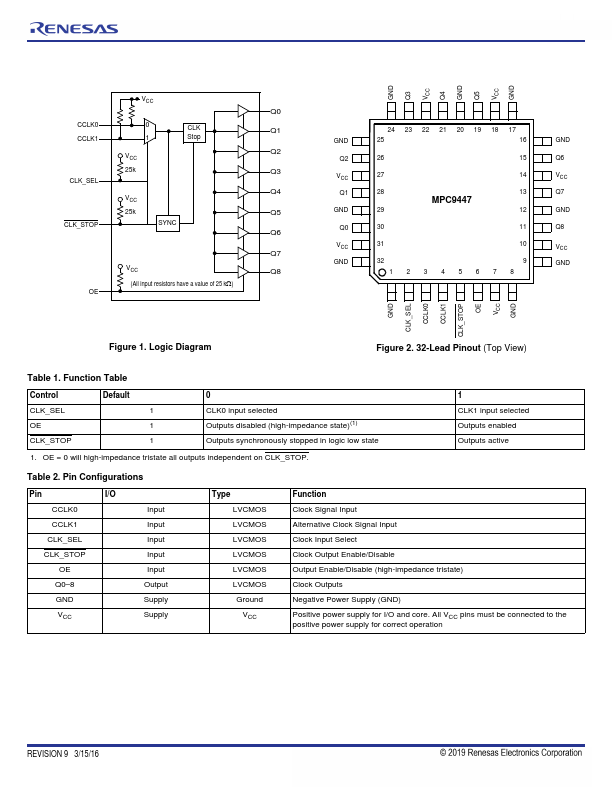
The Freescale Semiconductor, Inc. MPC9447 is a 3.3 V or 2.5 V compatible, 1:9 clock fanout buffer targeted for high performance clock tree applications. With output frequencies up to 350 MHz and output skews less than 150 ps, the device meets the needs of most demanding clock applications. Features • 9 LVCMOS Compatible Clock Outputs • 2 Selectable, LVCMOS Compatible Inputs • Maximum Clock Frequency of 350 MHz • Maximum Clock Skew of 150 ps • Synchronous Output Stop in Logic Low State Eliminates Output Runt Pulses • High-Impedance Output Control • 3.3 V or 2.
Published: |