HD74LV1GT125A Key Features
- The basic gate function is lined up as Renesas uni logic series
- Supplied on emboss taping for high-speed automatic mounting
- TTL patible input level. Supply voltage range : 3.0 to 5.5 V Operating temperature range : -40 to +85°C
- Logic-level translate function 3.0 V CMOS logic → 5.0 V CMOS logic (@VCC = 5.0 V) 1.8 V or 2.5 V CMOS logic → 3.3 V CMOS
- All inputs VIH (Max.) = 5.5 V (@VCC = 0 V to 5.5 V) All outputs VO (Max.) = 5.5 V (@VCC = 0 V, Output : Z)
- Output current ±6 mA (@VCC = 3.0 V to 3.6 V), ±12 mA (@VCC = 4.5 V to 5.5 V)
- All the logical input has hysteresis voltage for the slow transition
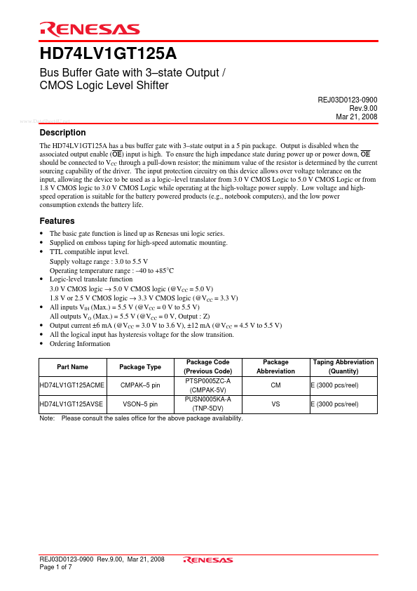
- Ordering Information
- HD74LV1GT125A
- HD74LV1GT125A