Description
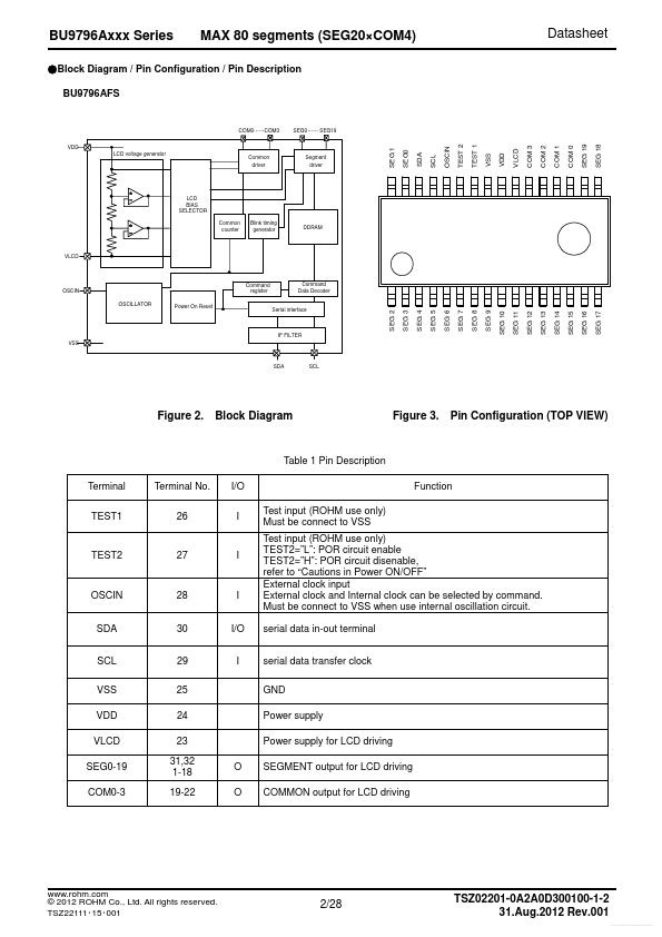
BU9796AFS
COM0……COM3 VDD LCD voltage generator Common driver
SEG0 …… SEG19
SEG 19 SEG 16
Segment driver
+ -
LCD BIAS SELECTOR Common counter Blink timing generator DDRAM
+ -
VLCD
OSCIN OSCILLATOR Power On Reset
Command register
Command Data Decoder
SEG 2
SEG 3
SEG 4
SEG 5
SEG 6
SEG 7
SEG 8
SEG 9
SEG 10
SEG 11
SEG 12
SEG 13
SEG 14
SEG 15
IF FILTER VSS
SDA
SCL
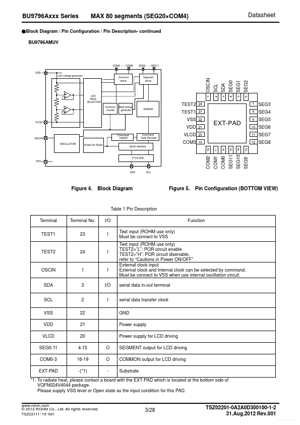
Figure 2. Block Diagram
Figure 3.
Pin Configuration (TOP VIEW)
Table 1 Pin Description Terminal TEST1 Termi
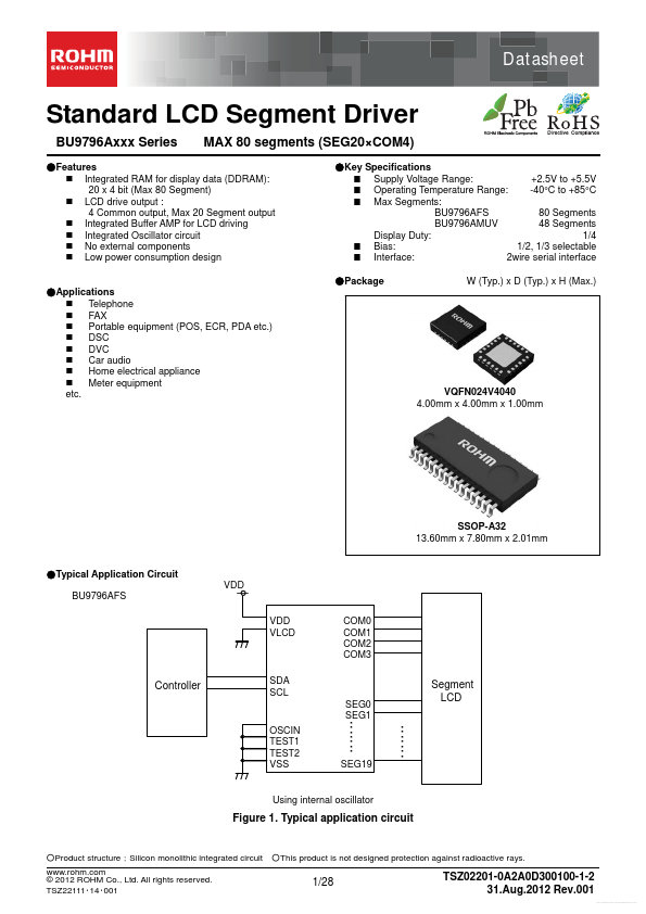
Features
- r>.
- Integrated RAM for display data (DDRAM): 20 x 4 bit (Max 80 Segment).
- LCD drive output : 4 Common output, Max 20 Segment output.
- Integrated Buffer AMP for LCD driving.
- Integrated Oscillator circuit.
- No external components.
- Low power consumption design
VQFN024V4040 4.00mm x 4.00mm x 1.00mm
SSOP-A32 13.60mm x 7.80mm x 2.01mm.
- Typical.