RDN120N25
RDN120N25 is Switching manufactured by ROHM.
Transistors
Switching (250V, 12A)
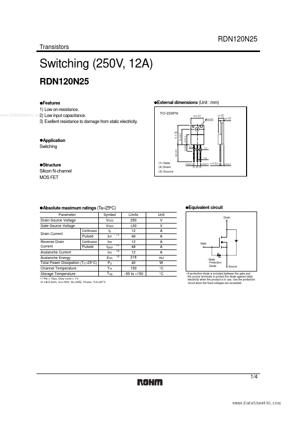
RDN120N25 z Features 1) Low on-resistance. .. 2) Low input capacitance. 3) Exellent resistance to damage from static electricity. z External dimensions (Unit : mm)
TO-220FN
+0.3 10.0
- 0.1 0.3 4.5 +
- 0.1
3.2±0.2
- 0.1
+0.2
0.4 15.0 +
- 0.2
12.0±0.2 z Application Switching
5.0±0.2 8.0±0.2
14.0±0.5
0.8 z Structure Silicon N-channel MOS FET
(1) Gate (2) Drain (3) Source
2.54±0.5
2.54±0.5 0.75
- 0.05
+0.1
2.6±0.5
(1) (2) (3) z Absolute maximum ratings (Ta=25°C)
Parameter Drain-Source Voltage Gate-Source Voltage Drain Current Reverse Drain Current Continuous Pulsed Continuous Pulsed Symbol VDSS VGSS ID IDP ∗1 IDR IDRP ∗1 IAS ∗2 EAS ∗2 PD Tch Tstg Limits 250 ±30 12 48 12 48 12 216 40 150
- 55 to +150 Unit V V A A A A A m J W °C °C z Equivalent circuit
Drain
Gate
Avalanche Current Avalanche Energy Total Power Dissipation (TC=25°C) Channel Temperature Storage Temperature
∗Gate Protection Diode
Source
∗1 Pw ≤ 10µs, Duty cycle ≤ 1% ∗2 L 2.4m H, VDD=50V, RG=25Ω, 1Pulse, Tch=25°C
∗A protection diode is included between the gate and the source terminals to protect the diode against static electricity when the product is in use. Use the protection circuit when the fixed voltages are exceeded.
1/4
Transistors z Electrical characteristics (Ta=25°C)
Parameter Gate-Source Leakage Drain-Source Breakdown Voltage Zero Gate Voltage Drain Current Gate Threshold Voltage Static Drain-Source On-State Resistance Symbol IGSS V(BR) DSS IDSS VGS (th) RDS (on) ⏐Yfs⏐ Ciss Coss Crss td (on) tr td (off) tf trr Qrr Qg Min. ⎯ 250 ⎯ 2.0 ⎯ 3.7 ⎯ ⎯ ⎯ ⎯ ⎯ ⎯ ⎯ ⎯ ⎯ ⎯ Typ. ⎯ ⎯ ⎯ ⎯ 0.16 6.1 1224 443 154 17 32 58 28 169 0.95 31 Max. ±10 ⎯ 25 4.0 0.21 ⎯ ⎯ ⎯ ⎯ ⎯ ⎯ ⎯ ⎯ ⎯ ⎯ ⎯ Unit µA V µA V Ω S p F p F p F ns ns ns ns ns µC n C Conditions VGS= ±30V, VDS=0V ID=250µA, VGS=0V VDS=250V, VGS=0V VDS=10V, ID=1m A ID=6A, VGS=10V VDS=10V, ID=6.0A VDS=10V VGS=0V f=1MHz ID=6.0A, VDD 100V VGS=10V RL=16.7Ω RGS=10Ω IDR=12A, VGS=0V di / dt=100A / µs...