SR502 THRU SR510
SCHOTTKY BARRIER RECTIFIERS
Reverse Voltage – 20 to 100 V
Forward Current – 5 A
Features
• Plastic package has Underwriters Laboratory
Flammability Classification 94V-0
• Metal silicon junction, majority carrier conduction
• Low power loss, high efficieny
• High current capability, low forward voltage drop
• For use in low voltage, high frequency inverters,
free wheeling, and polarity protection applications
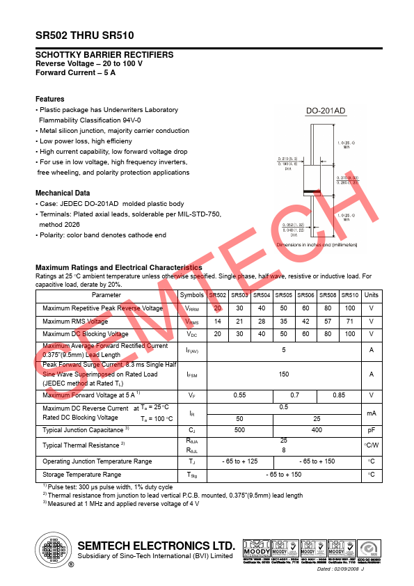
Mechanical Data
• Case: JEDEC DO-201AD molded plastic body
• Terminals: Plated axial leads, solderable per MIL-STD-750,
method 2026
• Polarity: color band denotes cathode end
HMaximum Ratings and Electrical Characteristics
CRatings at 25 OC ambient temperature unless otherwise specified. Single phase, half wave, resistive or inductive load. For
capacitive load, derate by 20%.
Parameter
Symbols SR502 SR503 SR504 SR505 SR506 SR508 SR510 Units
EMaximum Repetitive Peak Reverse Voltage
VRRM 20 30 40 50 60 80 100 V
Maximum RMS Voltage
VRMS 14 21 28 35 42 57 71 V
TMaximum DC Blocking Voltage
Maximum Average Forward Rectified Current
0.375"(9.5mm) Lead Length
MPeak Forward Surge Current, 8.3 ms Single Half
Sine Wave Superimposed on Rated Load
E(JEDEC method at Rated TL)
Maximum Forward Voltage at 5 A 1)
Maximum DC Reverse Current at Ta = 25 OC
SRated DC Blocking Voltage
Ta = 100 OC
VDC
IF(AV)
IFSM
VF
IR
20 30 40 50 60 80 100 V
5A
150 A
0.55 0.7 0.85 V
0.5
50 25
mA
Typical Junction Capacitance 3)
CJ 500
400 pF
Typical Thermal Resistance 2)
RθJA
RθJL
25
8
OC/W
Operating Junction Temperature Range
TJ - 65 to + 125
- 65 to + 150
OC
Storage Temperature Range
TStg
- 65 to + 150
1) Pulse test: 300 µs pulse width, 1% duty cycle
2) Thermal resistance from junction to lead vertical P.C.B. mounted, 0.375"(9.5mm) lead length
3) Measured at 1 MHz and applied reverse voltage of 4 V
OC
SEMTECH ELECTRONICS LTD.
Subsidiary of Sino-Tech International (BVI) Limited
®
Dated : 02/09/2008 J