MB84VD21191EM-70
MB84VD21191EM-70 is (MB84VD2118xEM-70 / MB84VD2119xEM-70) Stacked MCP (Multi-Chip Package) FLASH MEMORY manufactured by SPANSION.
- Part of the MB84VD21181EM-70 comparator family.
- Part of the MB84VD21181EM-70 comparator family.
..
FUJITSU SEMICONDUCTOR DATA SHEET
DS05-50307-1E
Stacked MCP (Multi-Chip Package) FLASH MEMORY & SRAM
16M (×8/×16) FLASH MEMORY & 4M (×8/×16) STATIC RAM
MB84VD2118XEM-70/MB84VD2119XEM-70 s Features
- Power Supply Voltage of 2.7 V to 3.3 V
- High Performance 70 ns maximum access time (Flash) 70 ns maximum access time (SRAM)
- Operating Temperature
- 40 °C to +85 °C
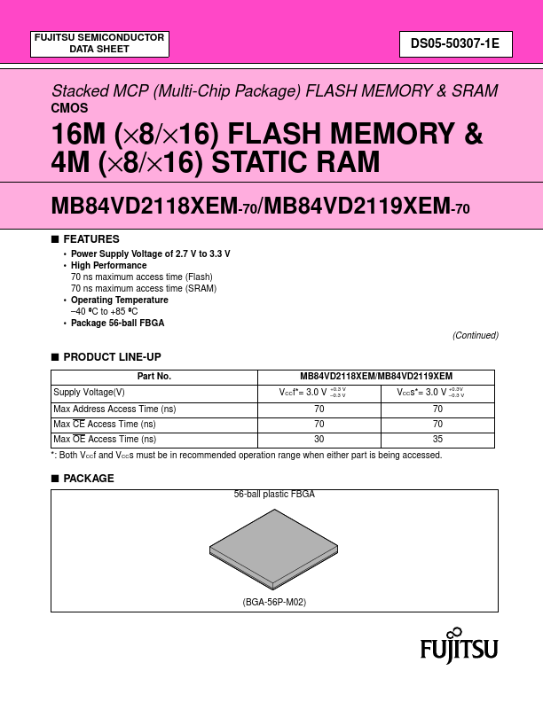
- Package 56-ball FBGA
CMOS
(Continued) s PRODUCT LINE-UP
Part No. Supply Voltage(V) Max Address Access Time (ns) Max CE Access Time (ns) Max OE Access Time (ns) MB84VD2118XEM/MB84VD2119XEM VCCf- = 3.0 V 70 70 30
+0.3 V
- 0.3 V
VCCs- = 3.0 V +0.3V
- 0.3 V 70 70 35
- : Both VCCf and VCCs must be in remended...