Datasheet4U Logo Datasheet4U.com

S25FL001D - (S25FL001D / S25FL002D) Flash Memory

Download the S25FL001D datasheet PDF. This datasheet also covers the S25FL002D variant, as both devices belong to the same (s25fl001d / s25fl002d) flash memory family and are provided as variant models within a single manufacturer datasheet.

Description

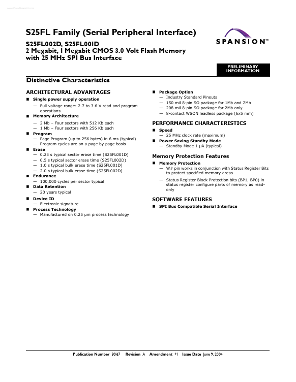
The S25FL002D and S25FL001D devices are 3.0 Volt (2.7 V to 3.6 V) single power supply Flash memory devices.

S25FL002D consists of four sectors, each with 512 Kb memory.

S25FL001D consists of four sectors, each with 256 Kb memory.

Features

  • Memory Protection.
  • W# pin works in conjunction with Status Register Bits to protect specified memory areas.
  • Status Register Block Protection bits (BP1, BP0) in status register configure parts of memory as readonly.

📥 Download Datasheet

Note: The manufacturer provides a single datasheet file (S25FL002D_SPANSION.pdf) that lists specifications for multiple related part numbers.

Full PDF Text Transcription (Reference)

The following content is an automatically extracted verbatim text from the original manufacturer datasheet and is provided for reference purposes only.

View original datasheet text
www.DataSheet4U.com S25FL Family (Serial Peripheral Interface) S25FL002D, S25FL001D 2 Megabit, 1 Megabit CMOS 3.0 Volt Flash Memory with 25 MHz SPI Bus Interface PRELIMINARY INFORMATION Distinctive Characteristics ARCHITECTURAL ADVANTAGES „ Single power supply operation — Full voltage range: 2.7 to 3.6 V read and program operations Memory Architecture — 2 Mb – Four sectors with 512 Kb each — 1 Mb – Four sectors with 256 Kb each Program — Page Program (up to 256 bytes) in 6 ms (typical) — Program cycles are on a page by page basis Erase — 0.25 s typical sector erase time (S25FL001D) — 0.5 s typical sector erase time (S25FL002D) — 1.0 s typical bulk erase time (S25FL001D) — 2.
Published: |