S29WS512N
S29WS512N is Migrating from the S71WS512N to the S71WS512P manufactured by SPANSION.
- Part of the S29WS512P comparator family.
- Part of the S29WS512P comparator family.
..
S71WS512N to S71WS512P
Migrating from the S71WS512N to the S71WS512P
Application Note by Daisuke Nakata
1. Introduction
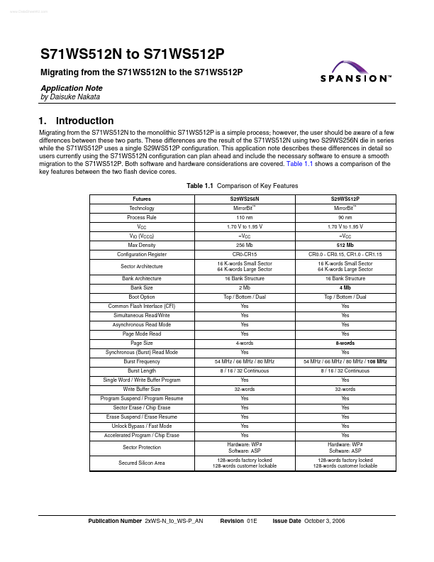
Migrating from the S71WS512N to the monolithic S71WS512P is a simple process; however, the user should be aware of a few differences between these two parts. These differences are the result of the S71WS512N using two S29WS256N die in series while the S71WS512P uses a single S29WS512P configuration. This application note describes these differences in detail so users currently using the S71WS512N configuration can plan ahead and include the necessary software to ensure a smooth migration to the S71WS512P. Both software and hardware considerations are...