FBGA-SD
FEATURES
- 2 die to 7 die stack with spacer capability
- 5 x 5mm to 23 x 23mm body size
- Package height at 1.0, 1.2, 1.4 and 1.7mm max.
- Flexible die stacking options (“pyramid,” “same die,” etc.)
- 0.5mm to 1.0mm ball pitch, Eutectic and Lead-free solder ball
- Flash/SRAM/PSRAM/Logic/Analog binations
- JEDEC standard package outlines
- Die thinning to 75um (3mils) capability
- Low loop wire bonding; reverse and die to die
- Up to 2mm die overhang per side
- Halogen-free and Low-K wafer patible BOM
- Ball counts up to 450 balls
DESCRIPTION
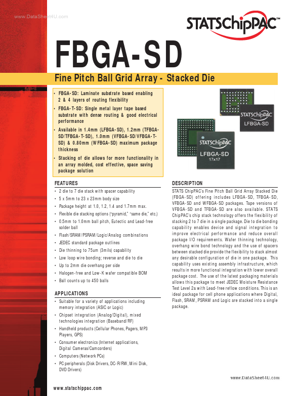
STATS Chip PAC’s Fine Pitch Ball Grid Array Stacked Die (FBGA-SD) offering includes LFBGA-SD, TFBGA-SD, VFBGA-SD and WFBGA-SD packages. Tape versions of VFBGA-SD and TFBGA-SD are also available. STATS Chip PAC’s chip stack technology offers the flexibility of stacking 2 to 7 die in a single package. Die to die bonding capability enables device and signal integration to improve electrical performance and reduce overall package I/O requirements....