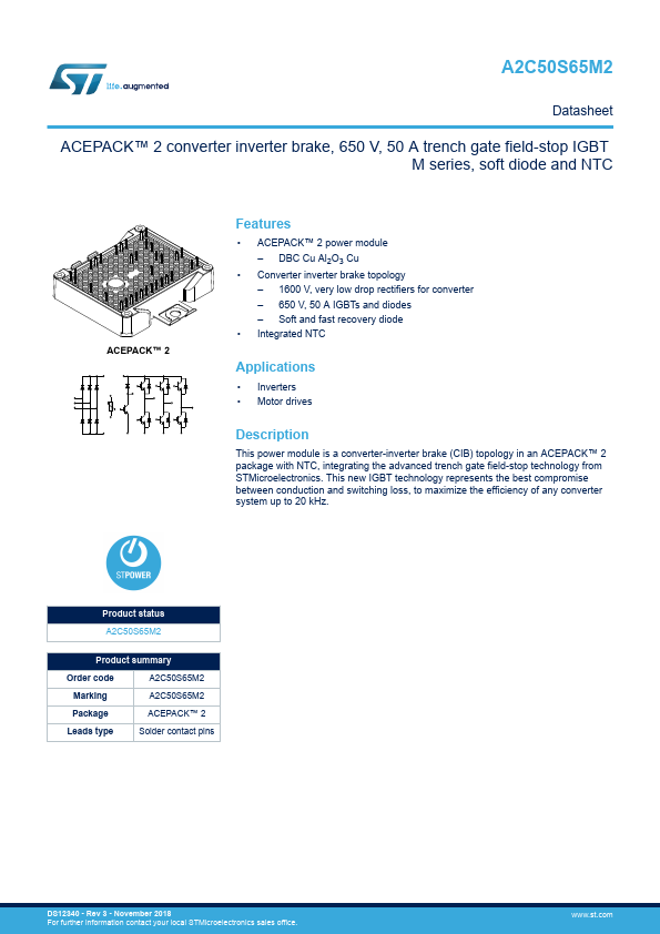
1 Electrical ratings
A2C50S65M2
Electrical ratings
1.1
1.1.1
Inverter stage
Limiting values at TJ = 25 °C, unless otherwise specified.
IGBTs
Table 1. Absolute maximum ratings of the IGBTs, inverter stage
Symbol
Description
VCES
Collector-emitter voltage (VGE = 0 V)
IC Continuous collector current (TC = 100 °C)
ICP(1)
Pulsed collector current (tp = 1 ms)
VGE Gate-emitter voltage
PTOT
Total power dissipation of each IGBT (TC = 25 °C, TJ = 175 °C)
TJMAX
Maximum junction temperature
TJop Operating junction temperature range under switching conditions
1. Pulse width limited by maximum junction temperature
Value
650
50
100
±20
208
175
-40 to 150
Unit
V
A
A
V
W
°C
°C
Symbol
V(BR)CES
VCE(sat)
(terminal)
VGE(th)
ICES
IGES
Cies
Coes
Cres
Qg
td(on)
tr
Eon(1)
Table 2. Electrical characteristics of the IGBTs, inverter stage
Parameter
Collector-emitter breakdown
voltage
Collector-emitter saturation
voltage
Gate threshold voltage
Collector cut-off current
Gate-emitter leakage current
Input capacitance
Output capacitance
Reverse transfer capacitance
Total gate charge
Turn-on delay time
Current rise time
Turn-on switching energy
Test conditions
IC = 1 mA, VGE = 0 V
VGE = 15 V, IC= 50 A
VGE = 15 V, IC = 50 A,
TJ = 150 ˚C
VCE = VGE, IC = 1 mA
VGE = 0 V, VCE = 650 V
VCE = 0 V, VGE = ±20 V
VCE = 25 V, f = 1 MHz,
VGE = 0 V
VCC = 520 V, IC = 50 A,
VGE = ±15 V
VCC = 300 V, IC = 50 A,
RG = 6.8 Ω, VGE = ±15 V,
di/dt = 2320 A/µs
Min.
650
Typ.
1.95
2.3
56
4150
170
80
150
147
17.5
0.147
Max.
Unit
V
2.3 V
V
7V
100 μA
±500 nA
pF
pF
pF
nC
ns
ns
mJ
DS12340 - Rev 3
page 2/16