Datasheet Summary
M24256-BW M24256-BR M24256-BF M24256-DR M24256-DF
256-Kbit serial I²C bus EEPROM
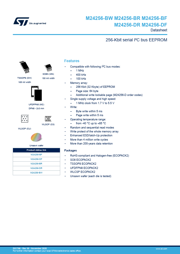
TSSOP8 (DW) 169 mil width
SO8N (MN) 150 mil width
UFDFPN8 (MC) DFN8
- 2x3 mm
WLSCP (CU)
WLSCP (CS)
Unsawn wafer Product status link
M24256-BF M24256-DF M24256-BR M24256-DR M24256-BW
Features
- patible with following I2C bus modes:
- 1 MHz
- 400 kHz
- 100 kHz
- Memory array:
- 256 Kbit (32 Kbyte) of EEPROM
- Page size: 64 byte
- Additional write lockable page (M24256-D order codes)
- Single supply voltage and high speed:
- 1 MHz clock from 1.7 V to 5.5 V
- Write:
- Byte write within 5 ms
- Page write within 5 ms
- Operating temperature range:
- from -40 °C up to +85 °C
- Random and...