P6NA60
DESCRIPTION
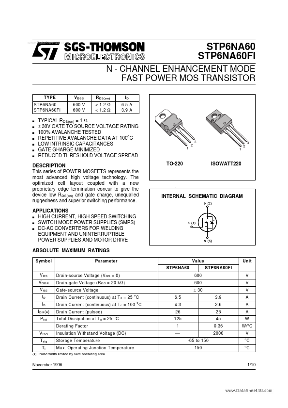
This series of POWER MOSFETS represents the most advanced high voltage technology. The optimized cell layout coupled with a new proprietary edge termination concur to give the device low RDS(on) and gate charge, unequalled ruggedness and superior switching performance. APPLICATIONS s HIGH CURRENT, HIGH SPEED SWITCHING s SWITCH MODE POWER SUPPLIES (SMPS) s DC-AC CONVERTERS FOR WELDING EQUIPMENT AND UNINTERRUPTIBLE POWER SUPPLIES AND MOTOR DRIVE ABSOLUTE MAXIMUM RATINGS
Symbol Parameter
ISOWATT220
INTERNAL SCHEMATIC DIAGRAM
Value STP6NA60 STP6NA60FI 600 600 ± 30 o
Unit
V DS V DGR V GS ID ID I DM (
- ) P tot V ISO T stg Tj
Drain-source Voltage (V GS = 0) Drain-gate Voltage (R GS = 20 k Ω ) Gate-source Voltage Drain Current (continuous) at T c = 25 C Drain Current (continuous) at T c = 100 o C Drain Current (pulsed) Total Dissipation at T c = 25 C Derating Factor Insulation Withstand Voltage (DC) Storage Temperature Max. Operating Junction Temperature o
V V V 3.9 2.6 26...