Datasheet Details
| Part number | P6NA60FP |
|---|---|
| Manufacturer | STMicroelectronics |
| File Size | 80.28 KB |
| Description | STP6NA60FP |
| Datasheet | P6NA60FP_STMicroelectronics.pdf |
|
|
|
Overview: .. 
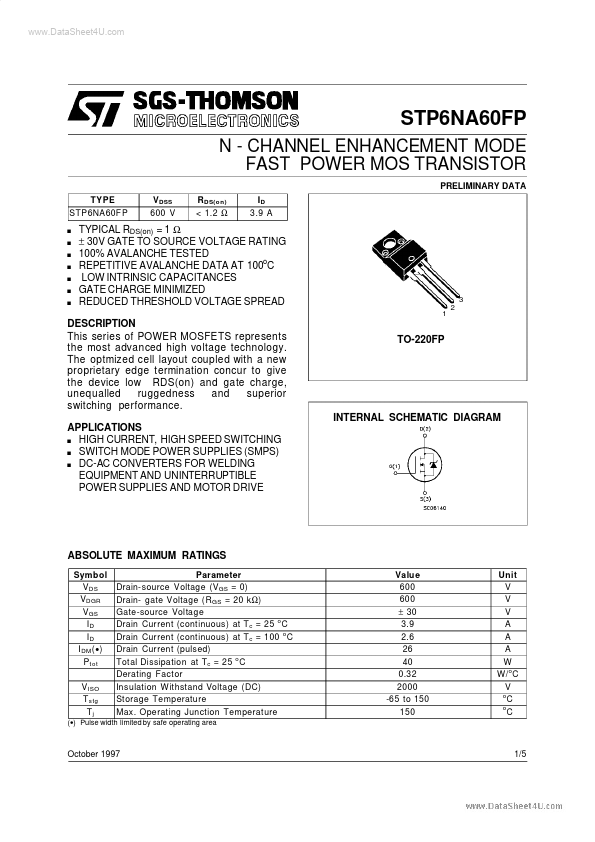
STP6NA60FP N - CHANNEL ENHANCEMENT MODE FAST POWER MOS TRANSISTOR PRELIMINARY DATA TYPE STP6NA60F P s s s s s s s V DSS 600 V R DS(on) < 1.2 Ω ID 3.
| Part number | P6NA60FP |
|---|---|
| Manufacturer | STMicroelectronics |
| File Size | 80.28 KB |
| Description | STP6NA60FP |
| Datasheet | P6NA60FP_STMicroelectronics.pdf |
|
|
|
This series of POWER MOSFETS represents the most advanced high voltage technology.
The optmized cell layout coupled with a new proprietary edge termination concur to give the device low RDS(on) and gate charge, unequalled ruggedness and superior switching performance.
APPLICATIONS s HIGH CURRENT, HIGH SPEED SWITCHING s SWITCH MODE POWER SUPPLIES (SMPS) s DC-AC CONVERTERS FOR WELDING EQUIPMENT AND UNINTERRUPTIBLE POWER SUPPLIES AND MOTOR DRIVE TO-220FP INTERNAL SCHEMATIC DIAGRAM ABSOLUTE MAXIMUM RATINGS Symbol V DS VDGR V GS ID ID I DM ( • ) P t ot V ISO T stg Tj Parameter Drain-source Voltage (V GS = 0) Drain- gate Voltage (R GS = 20 k Ω) Gate-source Voltage Drain Current (continuous) at T c = 25 o C o Drain Current (continuous) at T c = 100 C Drain Current (pulsed) Total Dissipation at Tc = 25 o C Derating Factor Insulation W ithstand Voltage (DC) St orage Temperature Max.
| Brand Logo | Part Number | Description | Manufacturer |
|---|---|---|---|
![]() |
P6NA60FI | STP6NA60FI | ST Microelectronics |
| Part Number | Description |
|---|---|
| P6NA60 | STP6NA60 |
| P6NB50FP | STP6NB50FP |
| P6NC60FP | STP6NC60FP |
| P6NK50Z | STP6NK50Z |
| P6NK60 | STP6NK60 |
| P6NK60Z | N-CHANNEL MOSFET |
| P6NK60ZFP | STP6NK60ZFP |
| P6NK60ZPF | STP6NK60ZPF |
| P6NK90ZFP | STP6NK90ZFP |