ST6G3240 Datasheet Text
.DataSheet.co.kr
ST6G3240
Dual supply level translator for dual memory cards (mini SD/micro SD + managed NAND)
Features
- -
- -
High speed: tPD (A to B) = 5 ns at TA = 85 °C with VCCA = 1.8 V, VCCBn = 3.0 V Low power dissipation: ICCA = ICCBn = 5 µA (max.) at TA = 85 °C Balanced propagation delays: tPLH ≈ tPHL Operating voltage range:
- VCCA (opr) = 1.4 to 3.6 V
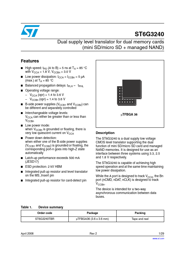
- VCCBn (opr) = 1.4 to 3.6 V B-side power supplies (VCCB1 and VCCB2) can be different and separately controlled Interchangeable voltage levels: VCCA can either be greater than or less than VCCBn Low power mode: when VCCBn is grounded or floating, there is very low quiescent current on VCCA Power down detection: when either one of the B-side power supplies (VCCB1 and VCCB2) is grounded or floating, the corresponding port-n goes into high-Z state automatically Latch-up performance exceeds 500 mA (JESD17) ESD protection: 2 kV HBM Integrated pull-up resistor and level translator on the MS_Insert pin Integrated pull-up resistor for card-detect pin μTFBGA 36
- -
- Description
The ST6G3240 is a dual supply low voltage CMOS level translator supporting the dual function of mini SD/micro SD card and managed NAND memories. It is designed for use as an interface between three systems using 3.3, 2.5 and 1.8 V respectively. The ST6G3240 is capable of achieving high speed operation and at the same time maintaining low power dissipation. While the A port is designed to track VCCA, the Bn port (nCMD, nDAT, nCLK) is designed to track VCCBn. The device is intended for a two-way asynchronous munication between data buses.
- -
- -
- Table 1.
Device summary
Order code ST6G3240TBR Package μTFBGA36 (3.6 x 3.6 mm) Packing Tape and reel
April 2008
Rev 2
1/29
.st. 29
Datasheet pdf
- http://..net/...