ST6G3244ME Overview
Key Specifications
Package: FCBGA
Mount Type: Surface Mount
Pins: 25
Operating Voltage: 1.8 V
Key Features
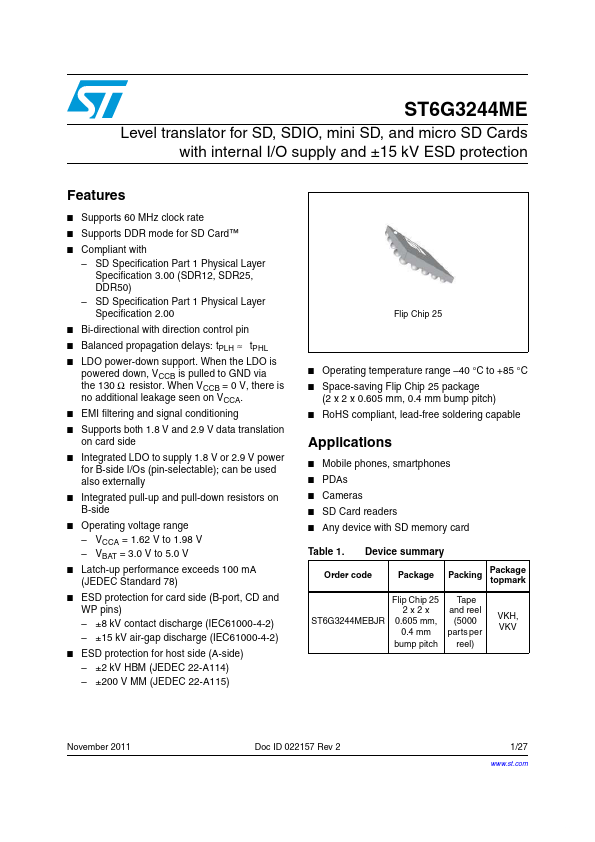
- Flip Chip 25
| Part | ST6G3244ME |
|---|---|
| Description | Level translator |
| Manufacturer | STMicroelectronics |
| Size | 741.30 KB |
Package: FCBGA
Mount Type: Surface Mount
Pins: 25
Operating Voltage: 1.8 V
| Seller | Inventory | Price Breaks | Buy |
|---|---|---|---|
| Newark | 100 | 1+ : 2.52 USD | View Offer |
| Arrow Electronics | 2087 | 1+ : 0.8336 USD 10+ : 0.8209 USD 25+ : 0.8083 USD 50+ : 0.7956 USD |
View Offer |
| Part Number | Manufacturer | Description |
|---|---|---|
| YF08E | Texas Instruments | Voltage Translator |
| HEF4104B | Nexperia | Quad low-to-high voltage translator |
| US5D304 | ultrasilicon | 4-Output Ultra-Low Additive Jitter Differential Clock Buffer/Level Translator |