STB100NF04
STB100NF04 is N-CHANNEL POWER MOSFET manufactured by STMicroelectronics.
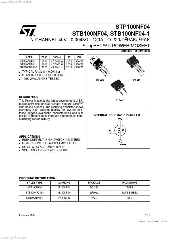
DESCRIPTION
This Power Mosfet is the latest development of STMicroelectronics unique “Single Feature
Size™” strip-based process. The resulting transistor shows extremely high packing density for low on-resistance, rugged avalanche characteristics and less critical alignment steps therefore a remarkable manufacturing reproducibility.
D2PAK
INTERNAL SCHEMATIC DIAGRAM
APPLICATIONS s HIGH CURRENT, HIGH SWITCHING SPEED s MOTOR CONTROL, AUDIO AMPLIFIERS s DC-DC & DC-AC CONVERTERS s SOLENOID AND RELAY DRIVERS
ORDERING INFORMATION
SALES TYPE STP100NF04 STB100NF04T4 STB100NF04-1 MARKING P100NF04 B100NF04 B100NF04 PACKAGE TO-220 D2PAK I2PAK PACKAGING TUBE TAPE & REEL TUBE
February 2002
1/15
Data Sheet 4 U .
..
STP100NF04, STB100NF04, STB100NF04-1
ABSOLUTE MAXIMUM RATINGS
Symbol VDS VDGR VGS ID (#) ID IDM (l) PTOT dv/dt (1) EAS (2) Tj Tstg Parameter Drain-source Voltage (VGS = 0) Drain-gate Voltage (RGS = 20 kΩ) Gate- source Voltage Drain Current (continuos) at TC = 25°C Drain Current (continuos) at TC = 100°C Drain Current (pulsed) Total Dissipation at TC = 25°C Derating Factor Peak Diode Recovery voltage slope Single Pulse Avalanche Energy Operating Junction Temperature Storage Temperature Value 40 40 ± 20 120 120 480 300 2 6 1.2 -55 to 175 Unit V V V A A A W W/°C V/ns J °C
(l) Pulse width limited by safe operating area (1) I SD ≤120A, di/dt ≤ 300A/µs, VDD ≤ V(BR)DSS, Tj ≤ TJMAX. (2) Starting T j = 25°C, I d = 60A, VDD=30 V (#) Current Limited by Package
THERMAL DATA
TO-220 / I2PAK / D2PAK Rthj-case Rthj-pcb Rthj-amb Tl Thermal Resistance Junction-case Max Thermal Resistance Junction-pcb Max Thermal Resistance Junction-ambient (Free air) Max Maximum Lead Temperature For Soldering Purpose 0.5 See Curve on page 6 62.5 300 °C/W °C/W °C/W °C
ELECTRICAL CHARACTERISTICS (TCASE =25°C UNLESS OTHERWISE SPECIFIED) ON/OFF
Symbol V(BR)DSS IDSS IGSS VGS(th) RDS(on) Parameter Drain-source Breakdown Voltage Zero Gate Voltage Drain Current (VGS = 0) Gate-body Leakage Current...