STL20NM20N
Overview
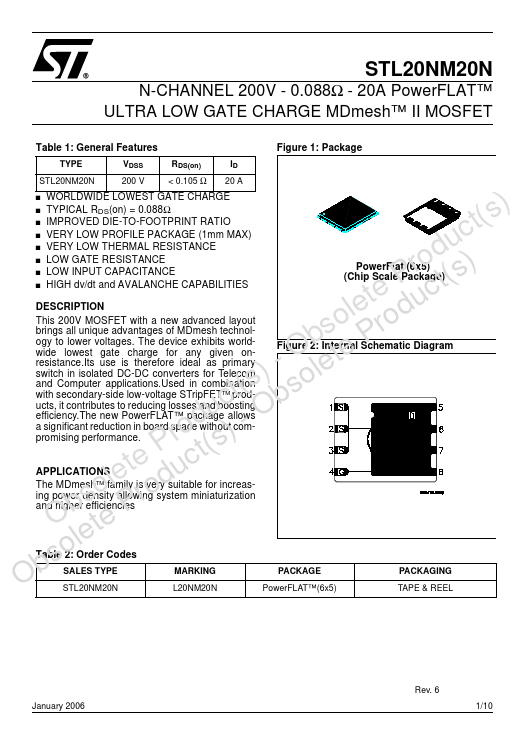
STL20NM20N N-CHANNEL 200V - 0.088Ω - 20A PowerFLAT™ ULTRA LOW GATE CHARGE MDmesh™ II MOSFET Table 1: General Features VDSS 200 V RDS(on) < 0.105 Ω ID 20 A Figure 1: Package TYPE STL20NM20N s s s s...
| Part | STL20NM20N |
|---|---|
| Description | N-CHANNEL MOSFET |
| Category | MOSFET |
| Manufacturer | STMicroelectronics |
| Size | 352.97 KB |
STL20NM20N N-CHANNEL 200V - 0.088Ω - 20A PowerFLAT™ ULTRA LOW GATE CHARGE MDmesh™ II MOSFET Table 1: General Features VDSS 200 V RDS(on) < 0.105 Ω ID 20 A Figure 1: Package TYPE STL20NM20N s s s s...
| Part Number | Manufacturer | Description |
|---|---|---|
| AP9563GH | Advanced Power Electronics Corp | P-CHANNEL ENHANCEMENT MODE POWER MOSFET |
| FCPF360N65S3R0L | onsemi | N-Channel MOSFET |
| A2SHB | HAOHAI | N-Channel MOSFET |