STP12NM60N
Features
..
Type
VDSS (@Tjmax) 650V 650V 650V 650V 650V
RDS(on) < 0.41Ω < 0.41Ω < 0.41Ω < 0.41Ω < 0.41Ω
3 12
STB12NM60N STB12NM60N-1 STF12NM60N STP12NM60N STW12NM60N
10A 10A 10A(1) 10A 10A
D²PAK
I²PAK
TO-247
3 1 2
3 1 2
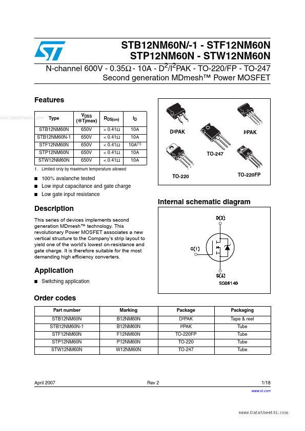
1. Limited only by maximum temperature allowed
- -
- 100% avalanche tested Low input capacitance and gate charge Low gate input resistance
TO-220
TO-220FP
Internal schematic diagram Description
This series of devices implements second generation MDmesh™ technology. This revolutionary Power MOSFET associates a new vertical structure to the pany’s strip layout to yield one of the world’s lowest on-resistance and gate charge. It is therefore suitable for the most demanding high efficiency converters.
Application
- Switching application
Order codes
Part number STB12NM60N STB12NM60N-1 STF12NM60N STP12NM60N STW12NM60N Marking B12NM60N B12NM60N F12NM60N P12NM60N W12NM60N Package D²PAK I²PAK TO-220FP TO-220 TO-247 Packaging Tape & reel Tube Tube Tube...