STP25NM60N
Overview
This series of devices is realized with the second generation of MDmesh™ technology. This revolutionary MOSFET associates a new vertical structure to the company’s strip layout to yield one of the world’s lowest on-resistance and gate charge.
- Limited only by maximum temperature allowed * *
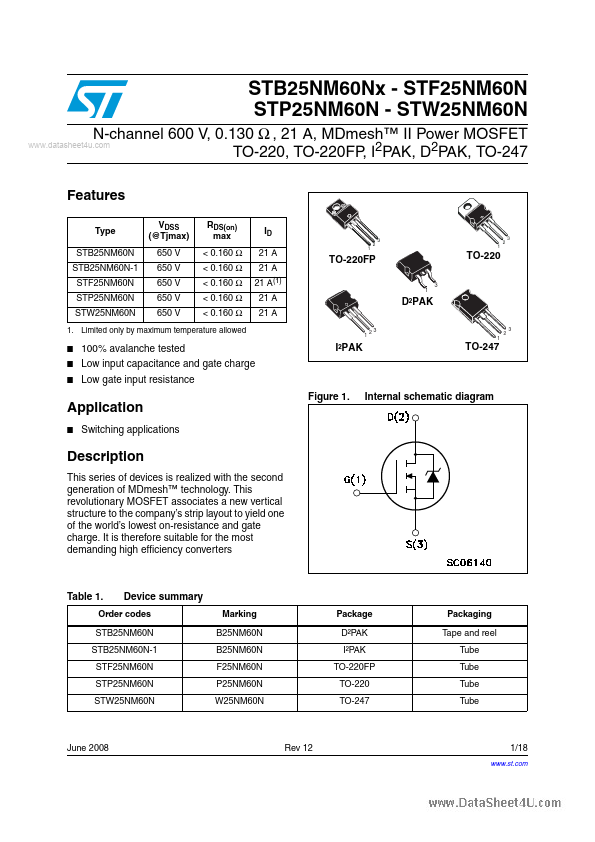
- 100% avalanche tested Low input capacitance and gate charge Low gate input resistance I²PAK TO-247 Figure
- Internal schematic diagram