Datasheet4U Logo Datasheet4U.com

STP5NB40 Datasheet N-CHANNEL ENHANCEMENT MODE PowerMESH MOSFET

Manufacturer: STMicroelectronics

General Description

P t(sUsing the latest high voltage MESH OVERLAY™ process, STMicroelectronics has designed an ad- te cvanced family of power MOSFETs with outstanding le uperformances.

The new patent pending strip layout so rodcoupled with the Company’s proprieraty edge termi- nation structure, gives the lowest RDS(on) per area, b Pexceptional avalanche and dv/dt capabilities and - O teunrivalled gate charge and switching characteris- tics.

t(s) oleAPPLICATIONS ss HIGH CURRENT, HIGH SPEED SWITCHING c bs SWITH MODE POWER SUPPLIES (SMPS) u Os DC-AC CONVERTERS FOR WELDING rod -EQUIPMENT P t(s)ABSOLUTE MAXIMUM RATINGS te cSymbol Parameter sole roduVDS b PVDGR O teVGS leID soID ObIDM (q) Drain-source Voltage (VGS = 0) Drain-gate Voltage (RGS = 20 kΩ) Gate- source Voltage Drain Current (continuos) at TC = 25°C Drain Current (continuos) at TC = 100°C Drain Current (pulsed) 3 2 1 TO-220 3 2 1 TO-220FP INTERNAL SCHEMATIC DIAGRAM Value STP5NB40 STP5NB40FP 400 400 ±30 4.7 4.7 (*) 3 3 (*) 19 19 (*) Unit V V V A A A PTOT Total Dissipation at TC = 25°C 80 30 W Derating Factor 0.64 0.24 W/°C dv/dt (1) Peak Diode Recovery voltage slope 4 4 V/ns VISO Insulation Withstand Voltage (DC) - 2500 V Tstg Storage Temperature –65 to 150 °C Tj Max.

Overview

STP5NB40 STP5NB40FP N-CHANNEL 400V - 1.47Ω - 
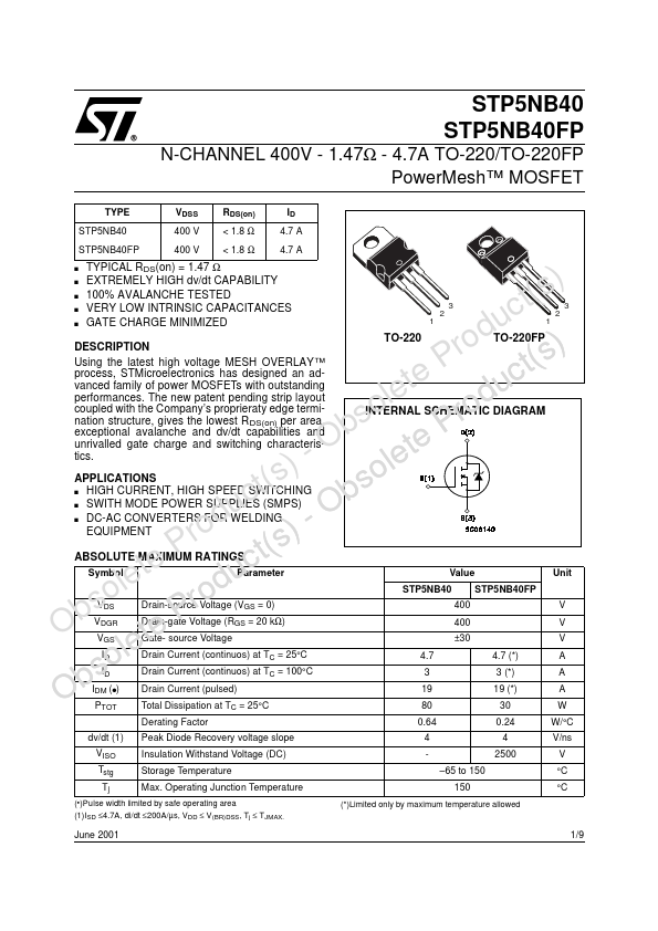
4.7A TO-220/TO-220FP PowerMesh™ MOSFET TYPE VDSS RDS(on) ID STP5NB40 400 V < 1.8 Ω 4.7 A STP5NB40FP 400 V < 1.8 Ω 4.7 A s TYPICAL RDS(on) = 1.