Datasheet Summary
..
STP9NK60ZFD
- STP9NK60ZFDFP STB9NK60ZFD
N-CHANNEL 600V
- 0.85Ω
- 7A TO-220/TO-220FP/D2PAK Fast Diode SuperMESH™ MOSFET
TARGET DATA TYPE STP9NK60ZFD STP9NK60ZFDFP STB9NK60ZFD s s s s s s
VDSS 600 V 600 V 600 V
RDS(on) < 0.95 Ω < 0.95 Ω < 0.95 Ω
ID 7A 7A 7A
Pw 104 W 32 W 104 W
3 1 2 s
TYPICAL RDS(on) = 0.85 Ω HIGH dv/dt CAPABILITY 100% AVALANCHE TESTED GATE CHARGE MINIMIZED LOW INTRINSIC CAPACITANCES VERY GOOD MANUFACTURING REPEATIBILITY FAST INTERNAL RECOVERY DIODE
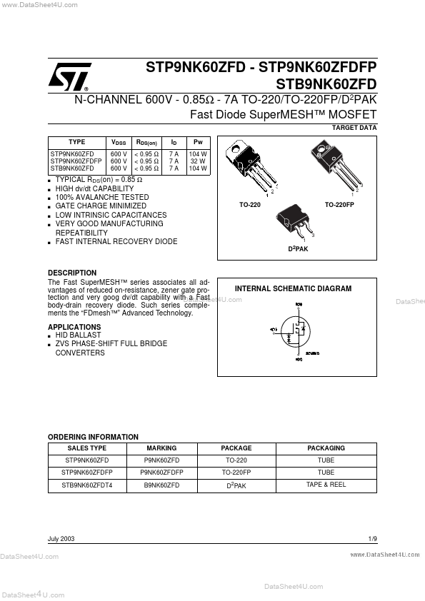
TO-220
TO-220FP
3 1
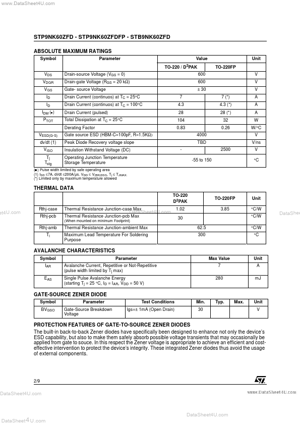
D2PAK
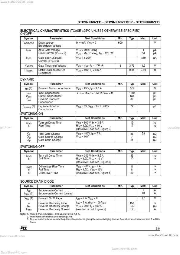
DESCRIPTION The Fast SuperMESH™ series associates all adINTERNAL SCHEMATIC DIAGRAM vantages of reduced on-resistance, zener gate protection and very goog dv/dt capability...