STP9NK60ZD
STP9NK60ZD is N-CHANNEL Power MOSFET manufactured by STMicroelectronics.
..
- STF9NK60ZD STB9NK60ZD
N-CHANNEL 600V
- 0.85Ω
- 7A TO-220/TO-220FP/D2PAK Super FREDMesh™ MOSFET
ADVANCED DATA TYPE STP9NK60ZD STF9NK60ZD STB9NK60ZD s s s s s s
VDSS 600 V 600 V 600 V
RDS(on) < 0.95 Ω < 0.95 Ω < 0.95 Ω
ID 7A 7A 7A
Pw 125 W 30 W 125 W
3 1 2
TYPICAL RDS(on) = 0.85 Ω VERY HIGH dv/dt CAPABILITY 100% AVALANCHE TESTED GATE CHARGE MINIMIZED LOW INTRINSIC CAPACITANCES FAST INTERNAL RECOVERY DIODE
TO-220
TO-220FP
3 1
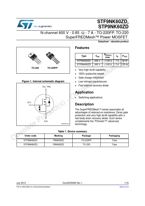
DESCRIPTION The Super FREDMesh™ series associates all advantages of reduced on-resistance, zener gate protection and very high dv/dt capability with a Fast body-drain recovery diode. Such series ple INTERNAL SCHEMATIC DIAGRAM ments the “FDmesh™” Advanced Technology. . APPLICATIONS s HID BALLAST s ZVS PHASE-SHIFT FULL BRIDGE CONVERTERS
D2PAK
Data Shee
ORDERING INFORMATION
SALES TYPE STP9NK60ZD STF9NK60ZD STB9NK60ZDT4 MARKING P9NK60ZD F9NK60ZD B9NK60ZD PACKAGE TO-220 TO-220FP D PAK
PACKAGING TUBE TUBE TAPE & REEL
January 2004
1/12
.
. Data Sheet 4 U .
..
- STF9NK60ZD
-...