Datasheet4U Logo Datasheet4U.com

STU7NB90 - N-channel Power MOSFET

General Description

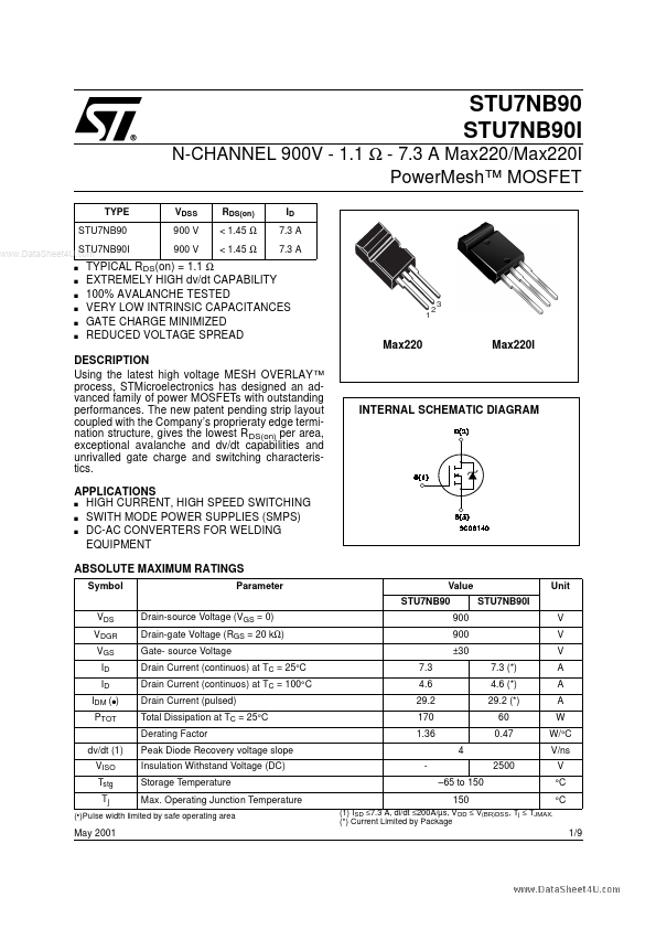
Using the latest high voltage MESH OVERLAY ™ process, STMicroelectronics has designed an advanced family of power MOSFETs with outstanding performances.

The new patent pending strip layout coupled with the Company’s proprieraty edge termination structure, gives the lowest R DS(on) per area, exceptional avalanche and dv/dt capabilities and unrivalled gate charge and switching characteristics.

APPLICATIONS s HIGH CURRENT, HIGH SPEED SWITCHING s SWITH MODE POWER SUPPLIES (SMPS) s DC-AC CONVERTERS FOR WELDING EQUIPMENT ABSOLUTE MAXIMUM RATINGS Symbol VDS VDGR VGS ID ID IDM (q) PTOT dv/dt (1) VISO Tstg Tj Parameter Drain-source Voltage (VGS = 0) Drain-gate Voltage (RGS = 20 kΩ) Gate- source Voltage Drain Current (continuos) at TC = 25°C Drain Current (continuos) at TC = 100°C Drain Current (pulsed) Total Dissipation at TC = 25°C Derating Factor Peak Diode Recovery voltage slope Insulation Withstand Voltage (DC) Storage Temperature Max.

Overview

N-CHANNEL 900V - 1.1 Ω - 7.3 A Max220/Max220I PowerMesh™ MOSFET TYPE STU7NB90 STU7NB90I www.DataSheet4U.com s s s s s s STU7NB90 STU7NB90I VDSS 900 V 900 V RDS(on) < 1.45 Ω < 1.45 Ω ID 7.3 A 7.3 A TYPICAL RDS(on) = 1.