Download K4S280832I Datasheet PDF
K4S280832I page 2
Page 2
K4S280832I page 3
Page 3

K4S280832I Key Features

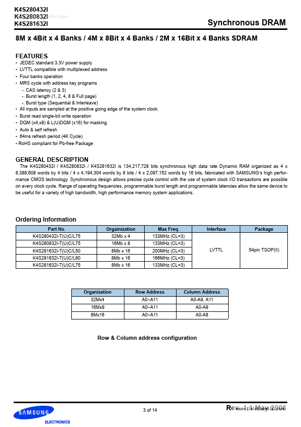
  • JEDEC standard 3.3V power supply LVTTL patible with multiplexed address Four banks operation MRS cycle with address key
  • All inputs are sampled at the positive going edge of the system clock
  • Burst read single-bit write operation
  • DQM (x4,x8) & L(U)DQM (x16) for masking
  • Auto & self refresh
  • 64ms refresh period (4K Cycle)
  • RoHS pliant for Pb-free Package

K4S280832I Description

Synchronous design allows precise cycle control with the use of system clock I/O transactions are possible on every clock cycle. Range of operating frequencies, programmable burst length and programmable latencies allow the same device to be useful for a variety of high bandwidth, high performance memory system applications. Ordering Information Part No.

K4S280832I Applications

  • Samsung Electronics reserves the right to change products or specification without notice