K7P403623B Description
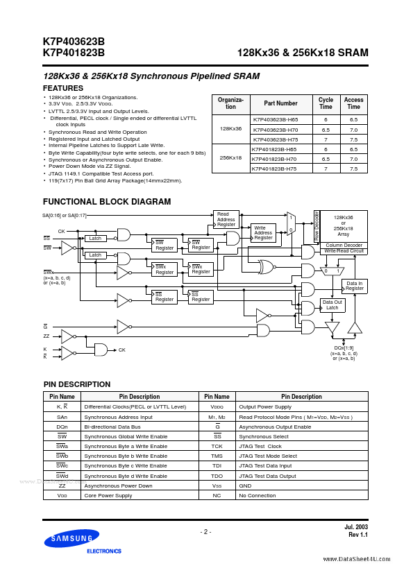
Pin Name K, K SAn DQn SW SWa SWb SWc SWd ZZ Pin Description Differential Clocks(PECL or LVTTL Level) Synchronous Address Input Bi-directional Data Bus Synchronous Global Write Enable Synchronous Byte a Write Enable Synchronous Byte b Write Enable Synchronous Byte c Write Enable Synchronous Byte d Write Enable Asynchronous Power Down Pin Name VDDQ M1, M2 G SS TCK TMS TDI TDO VSS NC Pin Description Output Power Supply...