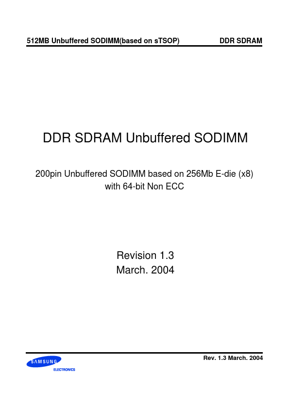
Part number:
M470L6423EN
Manufacturer:
Samsung semiconductor
File Size:
145.93 KB
Description:
512mb unbuffered sodimm.
M470L6423EN Features
* itions Parameter/Condition Input High (Logic 1) Voltage, DQ, DQS and DM signals Input Low (Logic 0) Voltage, DQ, DQS and DM signals. Input Differential Voltage, CK and CK input
M470L6423EN Datasheet (145.93 KB)
Datasheet Details
M470L6423EN
Samsung semiconductor
145.93 KB
512mb unbuffered sodimm.
📁 Related Datasheet
M470L1624FT0 DDR SDRAM SODIMM (Samsung semiconductor)
M470L3223DT0 256MB DDR SDRAM MODULE (Samsung semiconductor)
M470L3224BT0 256MB DDR SDRAM MODULE (Samsung semiconductor)
M470L3224FT0 DDR SDRAM SODIMM (Samsung semiconductor)
M470L3224FU0 DDR SDRAM SODIMM (Samsung semiconductor)
M470T2863FB3 200pin Unbuffered SODIMM (Samsung semiconductor)
M470T2863FB3-CE7 200pin Unbuffered SODIMM (Samsung semiconductor)
M470T2864FB3 200pin Unbuffered SODIMM (Samsung semiconductor)
M470L6423EN Distributor