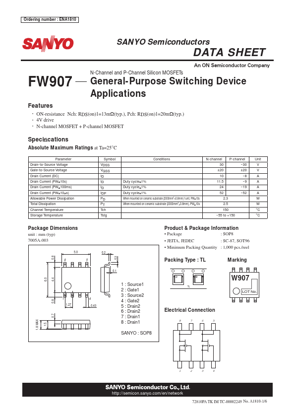
Datasheet4U Logo Datasheet4U.com

FW907 - N-Channel and P-Channel Silicon MOSFETs

Key Features

  • ON-resistance Nch: RDS(on)1=13mΩ(typ. ), Pch: RDS(on)1=20mΩ(typ. ).
  • 4V drive.
  • N-channel MOSFET + P-channel MOSFET Specifications Absolute Maximum Ratings at Ta=25°C Parameter Drain-to-Source Voltage Gate-to-Source Voltage Drain Current (DC) Drain Current (PW≤10s) Drain Current (PW≤100ms) Drain Current (PW≤10μs) Allowable Power Dissipation Total Dissipation Channel Temperature Storage Temperature Symbol VDSS VGSS ID ID ID IDP PD PT Tch Tstg Conditions Duty cycle≤1% D.

📥 Download Datasheet

Full PDF Text Transcription (Reference)

The following content is an automatically extracted verbatim text from the original manufacturer datasheet and is provided for reference purposes only.

View original datasheet text
Ordering number : ENA1810 FW907 SANYO Semiconductors DATA SHEET FW907 N-Channel and P-Channel Silicon MOSFETs General-Purpose Switching Device Applications Features • 
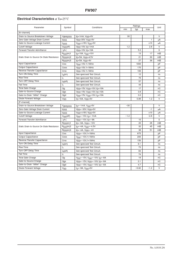
ON-resistance Nch: RDS(on)1=13mΩ(typ.), Pch: RDS(on)1=20mΩ(typ.) • 4V drive • N-channel MOSFET + P-channel MOSFET Specifications Absolute Maximum Ratings at Ta=25°C Parameter Drain-to-Source Voltage Gate-to-Source Voltage Drain Current (DC) Drain Current (PW≤10s) Drain Current (PW≤100ms) Drain Current (PW≤10μs) Allowable Power Dissipation Total Dissipation Channel Temperature Storage Temperature Symbol VDSS VGSS ID ID ID IDP PD PT Tch Tstg Conditions Duty cycle≤1% Duty cycle≤1% Duty cycle≤1% When mounted on ceramic substrate (2000mm2×0.8mm) 1unit, PW≤10s When mounted on ceramic substrate (2000mm2×0.