ATP214
ATP214 is N-Channel Silicon MOSFET manufactured by SANYO.
Features
- -
N-Channel Silicon MOSFET
General-Purpose Switching Device Applications
- -
ON-resistance RDS(on)1=6.2mΩ(typ.) 4V drive
Input Capacitance Ciss=4850p F(typ.) Halogen free pliance
Specifications
Absolute Maximum Ratings at Ta=25°C
Parameter Drain-to-Source Voltage Gate-to-Source Voltage Drain Current (DC) Drain Current (PW≤10μs) Allowable Power Dissipation Channel Temperature Storage Temperature Avalanche Energy (Single Pulse)
- 1 Avalanche Current
- 2 Symbol VDSS VGSS ID IDP PD Tch Tstg EAS IAV PW≤10μs, duty cycle≤1% Tc=25°C Conditions Ratings 60 ±20 75 225 60 150 --55 to +150 94 38 Unit V V A A W °C °C m J A
Note :
- 1 VDD=15V, L=100μH, IAV=38A
- 2 L≤100μH, Single pulse
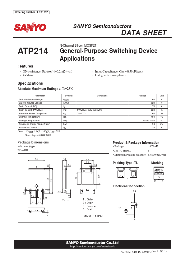
Package Dimensions unit : mm (typ) 7057-001
6.5 0.5 1.5 0.4
Product & Package Information
- Package : ATPAK
- JEITA, JEDEC :- Minimum Packing Quantity : 3,000 pcs./reel
4.6 2.6 0.4
Packing Type: TL
Marking
LOT No.
Electrical Connection
1.7 2 0.5 1 0.8 2.3 2.3 3 0.55 0.7 2,4
1 : Gate 2 : Drain 3 : Source 4 : Drain SANYO : ATPAK
3 http://semicon.sanyo./en/network
70710PA TK IM TC-00002343 No. A1712-1/4
Datasheet pdf
- http://..net/
.Data Sheet.co.kr
Electrical Characteristics at Ta=25°C
Parameter Drain-to-Source Breakdown Voltage Zero-Gate Voltage Drain Current Gate-to-Source Leakage Current Cutoff Voltage Forward Transfer Admittance Static Drain-to-Source On-State Resistance Input Capacitance Output Capacitance Reverse Transfer Capacitance Turn-ON Delay Time Rise Time Turn-OFF Delay Time Fall Time Total Gate Charge Gate-to-Source Charge Gate-to-Drain “Miller” Charge Diode Forward Voltage Symbol V(BR)DSS IDSS IGSS VGS(off) | yfs | RDS(on)1 RDS(on)2 RDS(on)3 Ciss Coss Crss td(on) tr td(off) tf Qg Qgs Qgd VSD Conditions ID=1m A, VGS=0V VDS=60V, VGS=0V VGS=±16V, VDS=0V VDS=10V, ID=1m A VDS=10V, ID=38A ID=38A, VGS=10V ID=19A, VGS=4.5V ID=10A, VGS=4V VDS=20V, f=1MHz VDS=20V, f=1MHz VDS=20V, f=1MHz See specified Test Circuit. See...