SGF9 Overview
Key Features
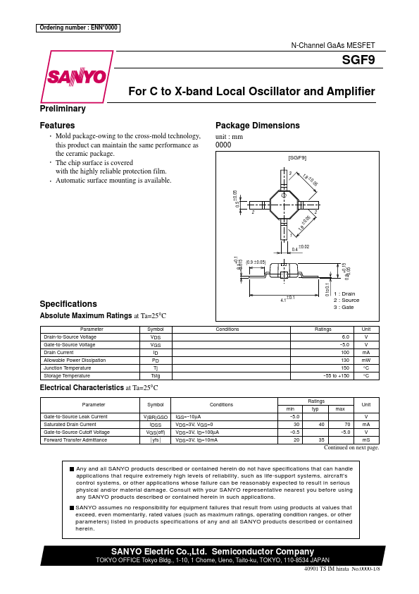
- Package Dimensions unit : mm 0000 [SGF9] 3
| Part | SGF9 |
|---|---|
| Description | For C to X-band Local Oscillator and Amplifier |
| Manufacturer | SANYO |
| Size | 66.79 KB |
| Part Number | Manufacturer | Description |
|---|---|---|
| G23N60UFD | Fairchild Semiconductor | SGF23N60UFD |
| SGFCF2002S-D | SUMITOMO | Plastic 2-stage GaN-HEMT |
| 5N150UF | Fairchild Semiconductor | SGF5N150UF |
| SGFM166C-D2 | Formosa MS | SMD Super Fast Rectifiers |
| SGFM164C-D2 | Formosa MS | SMD Super Fast Rectifiers |