S-89120A Description
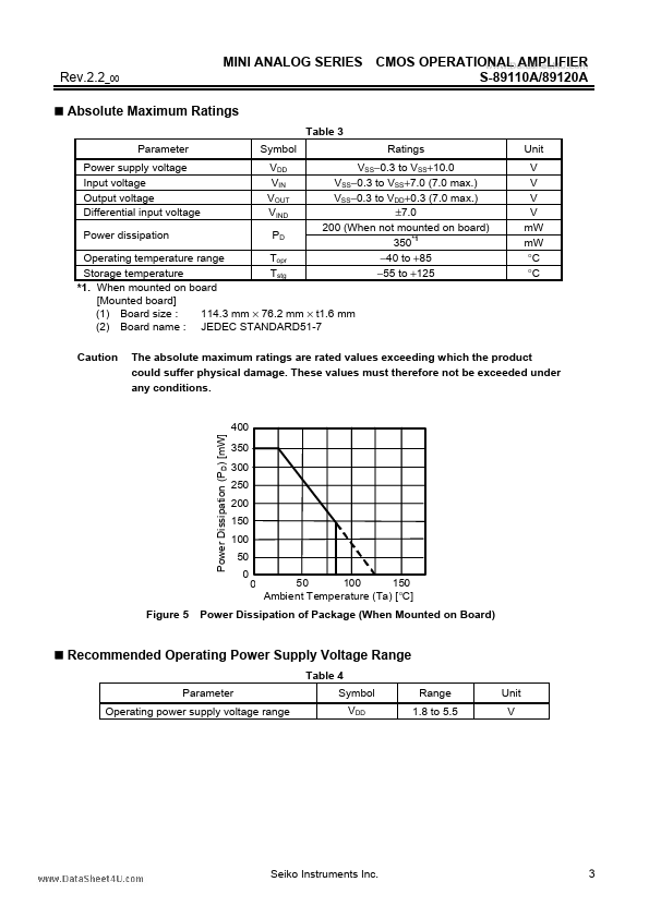
MINI ANALOG SERIES Rev.2.2_00 Ratings Table 3 Parameter Power supply voltage Input voltage Output voltage Differential input voltage Power dissipation Symbol VDD VIN VOUT VIND PD CMOS OPERATIONAL AMPLIFIER .. When mounted on board [Mounted board] (1) Board size : 114.3 mm × 76.2 mm × t1.6 mm (2) Board name.
S-89120A Key Features
- Features
- Application
- Package
- Product Name List