Datasheet4U Logo Datasheet4U.com

HYB39S16160CT-7 - 1M x 16 MBit Synchronous DRAM

Download the HYB39S16160CT-7 datasheet PDF. This datasheet also covers the HYB39S16160CT-6 variant, as both devices belong to the same 1m x 16 mbit synchronous dram family and are provided as variant models within a single manufacturer datasheet.

General Description

LVTTL-version: HYB 39S16160CT-6 HYB 39S16160CT-7 P-TSOPII-50 (400mil) P-TSOPII-50 (400mil) 166MHz 2B x 512k x 16 SDRAM 143MHz 2B x 512k x 16 SDRAM Pin Description and Pinouts: CLK CKE CS RAS CAS WE A0-A10 A11 (BS) Clock Input Clock Enable Chip Select Row Address Strobe Column Address Strobe Write

Key Features

  • ck, a RAS cycle starts. According to address data, a word line of the selected bank is activated and all of sense amplifiers associated to the word line a.

📥 Download Datasheet

Note: The manufacturer provides a single datasheet file (HYB39S16160CT-6_SiemensSemiconductor.pdf) that lists specifications for multiple related part numbers.

Full PDF Text Transcription (Reference)

The following content is an automatically extracted verbatim text from the original manufacturer datasheet and is provided for reference purposes only.

View original datasheet text
www.DataSheet4U.com HYB39S16160CT-6/-7 16MBit Synchronous DRAM 1M x 16 MBit Synchronous DRAM for High Speed Graphics Applications • High Performance: -
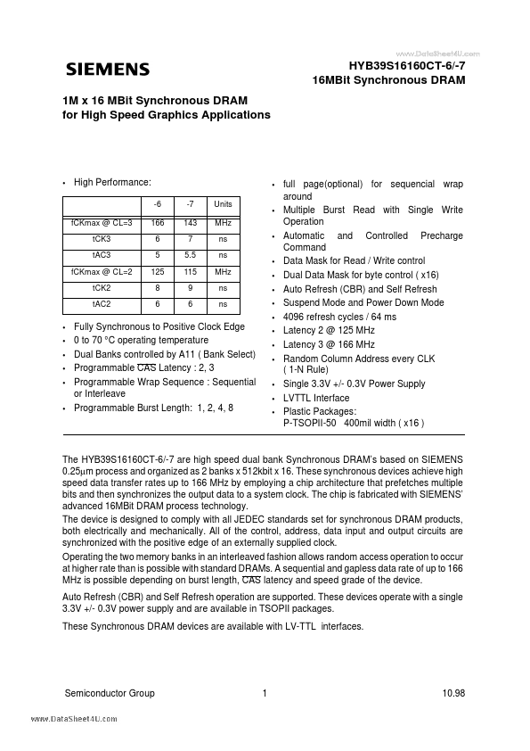
6 fCKmax @ CL=3 tCK3 tAC3 fCKmax @ CL=2 tCK2 tAC2 166 6 5 125 8 6 -7 143 7 5.5 115 9 6 Units MHz ns ns MHz ns ns • • • • • • • • full page(optional) for sequencial wrap around Multiple Burst Read with Single Write Operation Automatic Command and Controlled Precharge Data Mask for Read / Write control Dual Data Mask for byte control ( x16) Auto Refresh (CBR) and Self Refresh Suspend Mode and Power Down Mode 4096 refresh cycles / 64 ms Latency 2 @ 125 MHz Latency 3 @ 166 MHz Random Column Address every CLK ( 1-N Rule) Single 3.3V +/- 0.