HYB39S16160CT-8
Overview
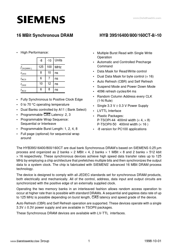
16 MBit Synchronous DRAM HYB 39S16400/800/160CT-8/-10 • High Performance: -8 -10 100 10 7 12 8 Units MHz ns ns ns ns fCK(MAX.) tCK3 tAC3 tCK2 tAC2 125 8 6 10 6 • Multiple Burst Read with Single ...
| Part | HYB39S16160CT-8 |
|---|---|
| Description | 16 MBit Synchronous DRAM |
| Manufacturer | Siemens Semiconductor Group |
| Size | 138.53 KB |
16 MBit Synchronous DRAM HYB 39S16400/800/160CT-8/-10 • High Performance: -8 -10 100 10 7 12 8 Units MHz ns ns ns ns fCK(MAX.) tCK3 tAC3 tCK2 tAC2 125 8 6 10 6 • Multiple Burst Read with Single ...
| Part Number | Manufacturer | Description |
|---|---|---|
| HM4864-2 | Hitachi Semiconductor | 65536 x 1-Bit DRAM |
| A3R12E40CBF | Zentel | 512Mb DDRII Synchronous DRAM |
| M12L128324A-6BIG2C | Elite Semiconductor Microelectronics Technology | 1M x 32 Bit x 4 Banks Synchronous DRAM |