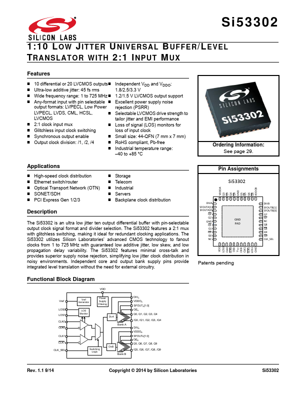
SI53302 Description
The Si53302 is an ultra low jitter ten output differential buffer with pin-selectable output clock signal format and divider selection.
SI53302 Key Features
- 10 differential or 20 LVCMOS outputs- Independent VDD and VDDO
- Ultra-low additive jitter: 45 fs rms
- Wide frequency range: 1 to 725 MHz
- 1.2/1.5 V LVCMOS output support
- Any-format input with pin selectable
- Excellent power supply noise output formats: LVPECL, Low Power rejection (PSRR)
- Selectable LVCMOS drive strength to tailor jitter and EMI performance
- 2:1 clock input mux
- Glitchless input clock switching
- Loss of signal (LOS) monitors for loss of input clock