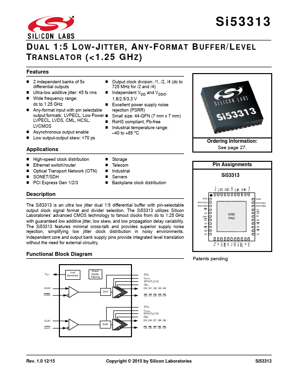
SI53313 Key Features
- 2 independent banks of 5x
- Ultra-low additive jitter: 45 fs rms
- Wide frequency range
- Independent VDD and VDDO: 1.8/2.5/3.3 V
- Excellent power supply noise
- Any-format input with pin selectable rejection (PSRR)
- Small size: 44-QFN (7 mm x 7 mm)
- RoHS pliant, Pb-free
- Industrial temperature range
- Asynchronous output enable