Download the 2N5463 datasheet PDF.
This datasheet also covers the 2N5460 variant, as both devices belong to the same p-channel jfet family and are provided as variant models within a single manufacturer datasheet.
Full PDF Text Transcription for 2N5463 (Reference)
Note: Below is a high-fidelity text extraction (approx. 800 characters) for
2N5463. For precise diagrams, and layout, please refer to the original PDF.
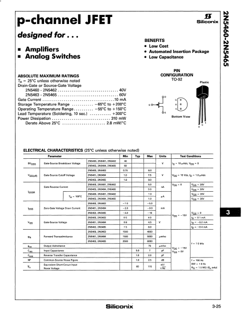
p-channel JFET designed for. • • • Amplifiers • Analog Switches ABSOLUTE MAXIMUM RATINGS TA = 25°C unless otherwise noted Drain-Gate or Source-Gate Voltage 2N5460 - 2N546...
View more extracted text
nless otherwise noted Drain-Gate or Source-Gate Voltage 2N5460 - 2N5462 ....•.......................... 40V 2N5463 - 2N5465 ..........................••... 60V Gate Current ................................•....10 rnA Storage Temperature Range ........... -65°C to +200°C Operating Temperature Range .••....... -55°C to +150°C Lead Temperature (Soldering. 10 sec.) ........... +300°C Power Dissipation .............................. 310 mW Derate Above 25°C ...................... 2.8 mW/oC .