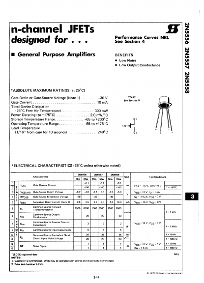
The following content is an automatically extracted verbatim text
from the original manufacturer datasheet and is provided for reference purposes only.
View original datasheet text
n-channel JFETs
designed for • • •
H~ Z UI
Performance Curves NRL See Section 4
UI UI
0-
• General Purpose Amplifiers
BENEFITS
• Low Noise
~
Z
UI UI
• Low Output Conductance
U....I.
~
UI
UI
*ABSOLUTE MAXIMUM RATINGS (at 25°C)
UI OG
Gate-Drain or Gate-Source Voltage (Note 1) ........ -30 V
Gate Current ............................... 10 mA Total Device Dissipation
(25°C Free Air Temperature) ................ 300mW Power Derating (to +175°C) ................ 2.0mWrC Storage Temperature Range .............. -65 to'+200°C
Operating Temperature Range ............ -65 to +175°C
Lead Temperature
(1/16" from case for 10 seconds) .............