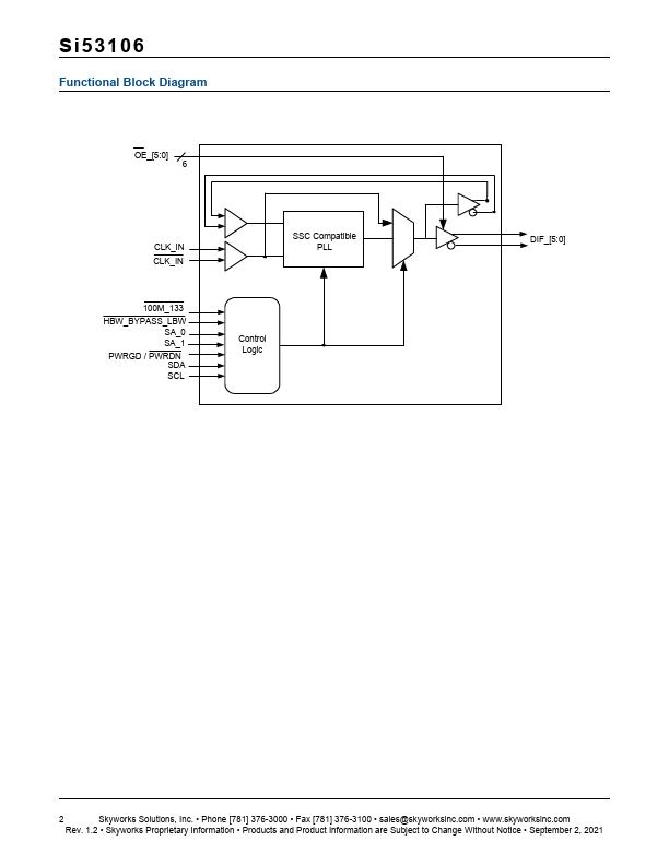
Datasheet Summary
S IX- O UTPUT P C I E G EN 3 B UFFER/ Z ERO D ELAY B UFFER
Features
- Six 0.7 V low-power, push-pull,
- Low phase jitter (Intel QPI, PCIe
HCSL-patible PCIe Gen 3
Gen 1/2/3/4 mon clock outputs pliant
- Individual OE HW pins for each
- Gen 3 SRNS pliant output clock
- PLL or bypass mode
- 100 MHz /133 MHz PLL
- Spread spectrum tolerable
- operation, supports PCIe and QPI
PLL bandwidth SW SMBUS programming overrides the latch
- -
- value from HW pin
1.05 to 3.3 V I/O supply voltage
50 ps output-to-output skew
Industrial Temperature:
- 40 to 85 °C
- SMBus address configurable to allow multiple buffers in a single
- -
40-pin QFN For higher output devices...