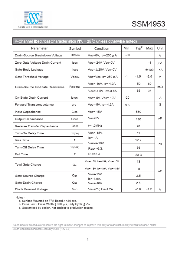
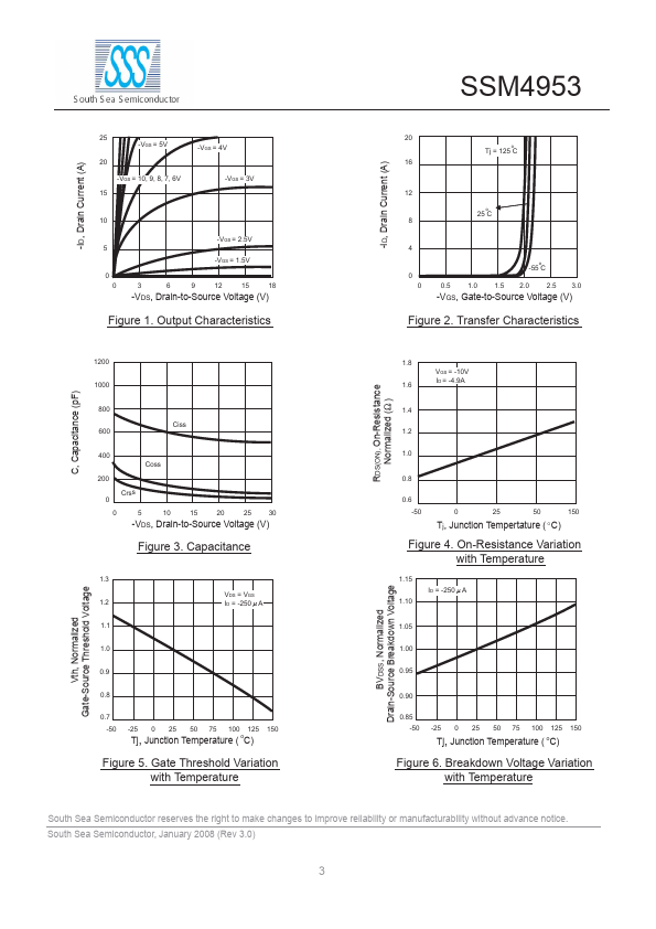
SSM4953 Description
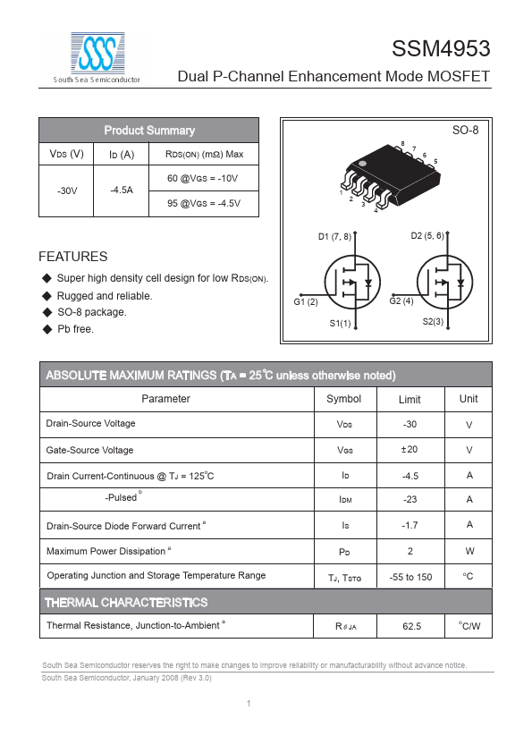
SSM4953 Dual P-Channel Enhancement Mode MOSFET Product Summary VDS (V) -30V SO-8 8 7 6 5 ID (A) -4.5A RDS(ON) (mΩ) Max 60 @VGS = -10V 1 95 @VGS = -4.5V 2 3 4 D1 (7, 8) D2 (5,.
SSM4953 is Dual P-Channel MOSFET manufactured by South Sea Semiconductor.
| Manufacturer | Part Number | Description |
|---|---|---|
| SSM4953M | P-channel Enhancement-mode Power MOSFET |
SSM4953 Dual P-Channel Enhancement Mode MOSFET Product Summary VDS (V) -30V SO-8 8 7 6 5 ID (A) -4.5A RDS(ON) (mΩ) Max 60 @VGS = -10V 1 95 @VGS = -4.5V 2 3 4 D1 (7, 8) D2 (5,.