TMPF16N25ZG
Overview
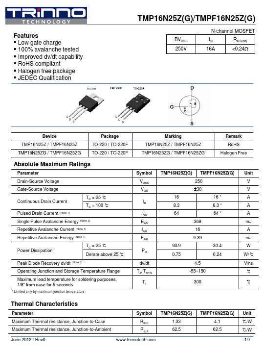
- Low gate charge
- 100% avalanche tested
- Improved dv/dt capability
- RoHS compliant
- Halogen free package
- JEDEC Qualification
| Part | TMPF16N25ZG |
|---|---|
| Description | N-channel MOSFET |
| Category | MOSFET |
| Manufacturer | TRinno |
| Size | 611.39 KB |
| Part Number | Manufacturer | Description |
|---|---|---|
| AP9563GH | Advanced Power Electronics Corp | P-CHANNEL ENHANCEMENT MODE POWER MOSFET |
| FCPF360N65S3R0L | onsemi | N-Channel MOSFET |
| A2SHB | HAOHAI | N-Channel MOSFET |