RN2130FV
TOSHIBA Transistor Silicon PNP Epitaxial Type (PCT Process)
Switching, Inverter Circuit, Interface Circuit and Driver Circuit Applications
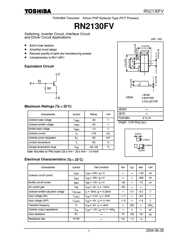
Unit : mm
0.22±0.05
0.32±0.05
Built-in bias resistors Simplified circuit design Reduced quantity of parts and manufacturing process plementary to RN1130FV
1.2±0.05 0.8±0.05
1.2±0.05 0.8±0.05 0.4 0.4
Equivalent Circuit
0.13±0.05
0.5±0.05
VESM
1.BASE 2.EMITTER 3.COLLECTOR
Maximum Ratings (Ta = 25°C)
JEDEC
―
Characteristic
Symbol
Rating
Unit
JEITA
―
Collector-base voltage Collector-emitter voltage
TOSHIBA
2-1L1A
VCBO
- 50
Weight : 0.0015mg (typ.)
VCEO
- 50
Emitter-base voltage
VEBO
- 10
Collector...