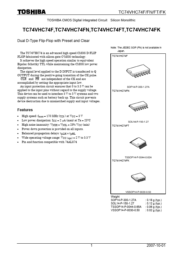
TC74VHC74FN Overview
Key Specifications
Package: SOP
Mount Type: Surface Mount
Pins: 14
Operating Voltage: 3.3 V
Key Features
- High speed: fmax = 170 MHz (typ.) at VCC = 5 V
- Low power dissipation: ICC = 2 μA (max) at Ta = 25°C
- High noise immunity: VNIH = VNIL = 28% VCC (min)
- Power down protection is provided on all inputs
- Balanced propagation delays: tpLH ∼- tpHL