TC78S122FNG Overview
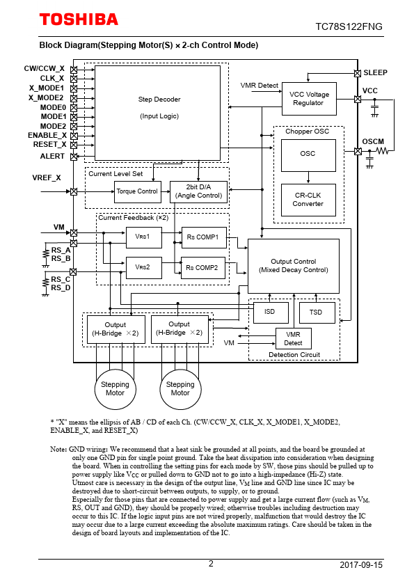
TC78S122FNG TOSHIBA CD Process Integrated Circuit Silicon Monolithic TC78S122FNG PWM Chopper Type Dual-Stepping Motor Driver The TC78S122FNG is a PWM chopper type dual-stepping motor driver. Two stepping motor drivers can drive up to four brushed DC motors. Incorporating two pairs of H-bridge drivers, the TC78S122FNG can drive two DC motors or a single stepping motor.
TC78S122FNG Key Features
- Single-chip motor driver for bipolar stepping motor control
- Monolithic IC structured by CD process
- Low ON-resistance: Ron = 0.6 Ω In large mode, ON-resistance of bined H-bridges (Ron) is 0.3 Ω
- Over-current detection (ISD), thermal shutdown (TSD) and VM power-on reset circuits
- Since the IC incorporates the VCC regulator for internal circuit operation, an external power supply (5 V) is not requir
- Package:HTSSOP48
- Maximum output withstand voltage: 40 V (max)
- Output current: 2.0 A (max) in DC Motor (S) mode; 1.5 A (max) in Stepping Motor (S) mode
- Chopping frequency can be set by external capacitor and resistor. High-speed chopping is possible at 100 kHz or higher
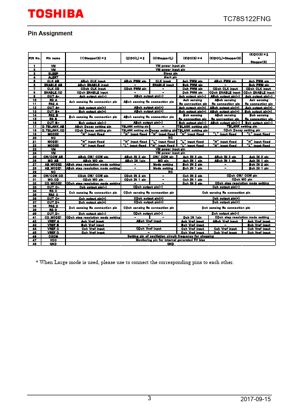
- "X" means the ellipsis of AB / CD of each Ch. (CW/CCW_X, CLK_X, X_MODE1, X_MODE2, ENABLE_X, and RESET_X)