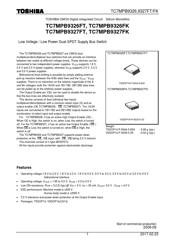
TC7MPB9326,9327FT/FK
TOSHIBA CMOS Digital Integrated Circuit Silicon Monolithic
TC7MPB9326FT, TC7MPB9326FK
TC7MPB9327FT, TC7MPB9327FK
Low Voltage / Low Power Dual SPDT Supply Bus Switch
The TC7MPB9326 and TC7MPB9327 are CMOS dual
multiplexer/demultiplexer bus switches that can provide an interface
between two nodes at different voltage levels. These devices can be
connected to two independent power supplies. VCCA supports 1.8 V,
2.5 V and 3.3 V power supplies, whereas VCCB supports 2.5 V, 3.3 V
and 5.0 V power supplies.
Bidirectional level-shifting is possible by simply adding external
pull-up resistors between the A/Bn data lines and the VCCA / VCCB
supplies. There is no restriction on the relative magnitude of the A
and Bn voltages; both the 1A/2A and 1B1/1B2 ,2B1/2B2 data lines
can be pulled up to the arbitrary power supplies.
The Output Enable pin (OE) can be used to disable the device so
that the bus lines are effectively isolated.
This device consists of dual individual two-inputs
multiplexer/demultiplexer with a common select input (S) and an
output enable (OE:TC7MPB9326, OE :TC7MPB9327). The 1A/2A
inputs are connected to 1B1/1B2 and 2B1/2B2 outputs based on the
combination of select input and output enable.
For TC7MPB9326, it has an active high Output Enable (OE) :
When OE is High, the switch is on; when Low, the switch is turned
off. For the TC7MPB9327, it has an active low Output Enable ( OE ) :
When OE is Low, the switch is turned on; when OE is High, the
switch is off.
The TC7MPB9326 and TC7MPB9327 supports power-down
protection at the OE , OE input, with OE , OE being 5.5 V tolerant.
The channels consist of n-type MOSFETs.
All the inputs provide protection against electrostatic discharge.
TC7MPB9326FT,TC7MPB9327FT
TC7MPB9326FK,TC7MPB9327FK
Weight
TSSOP14-P-0044-0.65A
VSSOP14-P-0030-0.50
: 0.06 g (typ.)
: 0.02 g (typ.)
Features
• Operating voltage:1.8 V to 2.5 V, 1.8 V to 3.3 V, 1.8 V to 5.0 V, 2.5 V to 3.3 V, 2.5 V to 5.0 V or 3.3 V to 5.0 V
bidirectional interface
• Operating voltage: VCCA = 1.65 to 5.0 V, VCCB = 2.3 to 5.5 V
• Low ON-resistance: RON = 5.0 Ω (typ.)@ VIS = 0 V, IIS = 30 mA, VCCA= 3.0 V , VCCB = 4.5 V
• ESD performance: Machine model ≥ ±200 V
Human body model ≥ ±2000 V
• 5.5 V tolerance and power-down protection at the Output Enable input.
• Packages: TSSOP14, VSSOP14(US14)
Start of commercial production
2009-09
1
2017-02-23