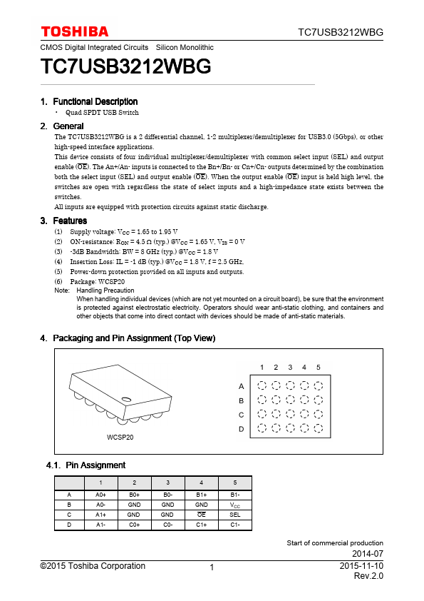
TC7USB3212WBG Overview
Key Specifications
Mount Type: Surface Mount
Operating Voltage: 1.8 V
Max Voltage (typical range): 1.95 V
Min Voltage (typical range): 1.65 V
Key Features
- Marking TC7USB3212WBG
| Part | TC7USB3212WBG |
|---|---|
| Description | Quad SPDT USB Switch |
| Manufacturer | Toshiba |
| Size | 245.49 KB |
Mount Type: Surface Mount
Operating Voltage: 1.8 V
Max Voltage (typical range): 1.95 V
Min Voltage (typical range): 1.65 V
| Seller | Inventory | Price Breaks | Buy |
|---|---|---|---|
| Avnet | 0 | - | View Offer |
| Microchip USA | 119 | 600+ : 4.874545 USD 1000+ : 4.874545 USD 10000+ : 4.874545 USD |
View Offer |
| Part Number | Manufacturer | Description |
|---|---|---|
| SW-331 | Tyco Electronics | Matched GaAs SPDT Switch |
| B3045G | onsemi | Switch-mode Power Rectifiers |
| DK1203 | Dongke Semiconductor | AC-DC Switch Mode Power controller |