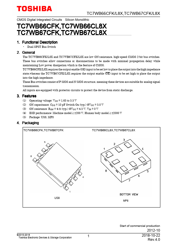
Datasheet4U Logo Datasheet4U.com

TC7WB66CFK - Dual SPST Bus Switch

General Description

2.

The TC7WB66CFK/L8X and TC7WB67CFK/L8X are low ON-resistance, high-speed CMOS 2-bit bus switches.

Key Features

  • (1) Operating voltage: VCC = 1.65 to 5.5 V (2) ON capacitance: CI/O = 10 pF Switch On (typ. ) @VCC = 5.0 V (3) ON resistance: RON = 4 Ω (typ. ) @VCC = 4.5 V, VIS = 0 V (4) ESD performance: Machine model ≥ ±200 V, Human body model ≥ ±2000 V (5) Package: US8, MP8 4. Packaging TC7WB66CFK,TC7WB67CFK TC7WB66CL8X,TC7WB67CL8X US8 ©2015-2018 Toshiba Electronic Devices & Storage Corporation 1 MP8 Start of commercial production 2012-10 2018-10-22 Rev.4.0 5. Pin Assignment TC7WB66CFK TC7WB66CFK/L8X,T.

📥 Download Datasheet

Full PDF Text Transcription for TC7WB66CFK (Reference)

Note: Below is a high-fidelity text extraction (approx. 800 characters) for TC7WB66CFK. For precise diagrams, and layout, please refer to the original PDF.

TC7WB66CFK/L8X,TC7WB67CFK/L8X CMOS Digital Integrated Circuits Silicon Monolithic TC7WB66CFK,TC7WB66CL8X TC7WB67CFK,TC7WB67CL8X 1. Functional Description • Dual SPST Bus ...

View more extracted text
CL8X TC7WB67CFK,TC7WB67CL8X 1. Functional Description • Dual SPST Bus Switch 2. General The TC7WB66CFK/L8X and TC7WB67CFK/L8X are low ON-resistance, high-speed CMOS 2-bit bus switches. These bus switches allow connections or disconnections to be made with minimal propagation delay while maintaining Low power dissipation which is the feature of CMOS. TC7WB66CFK/L8X requires the output enable (OE) input to be set low to place the output into the high impedance state,whereas the TC7WB67CFK/L8X requires the output enable (OE) input to be set high to place the output into the high impedance.