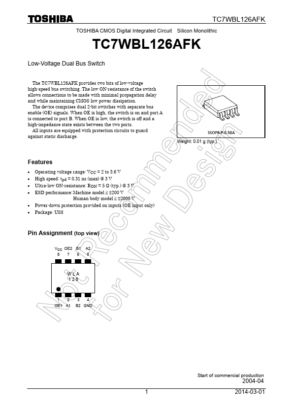
Datasheet4U Logo Datasheet4U.com

TC7WBL126AFK - Low-Voltage Dual Bus Switch

Key Features

  • Operating voltage range: VCC = 2 to 3.6 V.
  • High speed: tpd = 0.31 ns (max) @ 3 V.
  • Ultra-low ON-resistance: RON = 5 Ω (typ. ) @ 3 V.
  • ESD performance: Machine model ≥ ±200 V Human body model ≥ ±2000 V.
  • Power-down protection provided on inputs (OE input only).
  • Package: US8 Pin Assignment (top view) VCC OE2 B1 A2 8765 WLA 126 12 34 OE1 A1 B2 GND Start of commercial production 2004-04 1 2014-03-01 Truth Table Inputs OE H L Function A port.

📥 Download Datasheet

Full PDF Text Transcription (Reference)

The following content is an automatically extracted verbatim text from the original manufacturer datasheet and is provided for reference purposes only.

View original datasheet text
TC7WBL126AFK TOSHIBA CMOS Digital Integrated Circuit Silicon Monolithic TC7WBL126AFK Low-Voltage Dual Bus Switch The TC7WBL126AFK provides two bits of low-voltage high-speed bus switching. The low ON-resistance of the switch allows connections to be made with minimal propagation delay and while maintaining CMOS low power dissipation. The device comprises dual 2-bit switches with separate bus enable (OE) signals. When OE is high, the switch is on and port A is connected to port B. When OE is low, the switch is off and a high-impedance state exists between the two ports. All inputs are equipped with protection circuits to guard against static discharge. Weight: 0.01 g (typ.) Features • Operating voltage range: VCC = 2 to 3.6 V • High speed: tpd = 0.